
User's Manual


User Manual
Version 01.00
2011-03-31
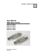
USB radio sticks deRFusb
dresden elektronik
ingenieurtechnik gmbh
Enno-Heidebroek-Str. 12
01237 Dresden / Germany
Tel.: 0351 – 31 85 00
Fax: 0351 – 3 18 50 10
wireless@dresden-elektronik.de
www.dresden-elektronik.de
Page 6 of 22
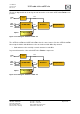
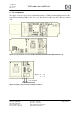
The block diagram below shows layout and interaction of the main deRFusb-23E00/06 com-
ponents:
VCC
ATSAM3S4BA AT86RF231 Chip antenna
2 GByte Flash
JTAG
DBGU
USB
VUSB
4.5 .. 5.5V
SPI
VCC
3.3V
MMC
Option:
Figure 1: block diagram deRFusb-23E00 / 06
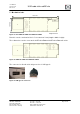
The deRFusb-13E00 and deRFusb-13E06 offer the same features like the deRFusb-23E00
/06 except the built-in Sub-GHz transceiver and onboard Sub-GHz chip antenna.
• Onboard transceiver and chip ceramic antenna for Sub-GHz
Layout and interaction of the main deRFusb-13E00/06 components:
VCC
ATSAM3S4BA AT86RF212 Chip antenna
2 GByte Flash
JTAG
DBGU
USB
VUSB
4.5 .. 5.5V
SPI
VCC
3.3V
MMC
Option:
Figure 2: block diagram deRFusb-13E00 / 06