
User Manual


datasheet
Version 0.9
2017-09-13
deRFsamR21E-23S00/-23S20 datasheet
www.dresden-elektronik.de
Page 9 of 36
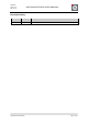
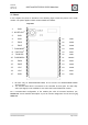
4. Pinout
In this chapter the pinout is described. The following figure shows the pinout of the radio
module. The pinout applies to both variants 23S00 and 23S20.
Top-View
1
GND
2
NC/RF-OUT
1
3
GND
4
GND
27
GND
5
PA14
26
PA09
6
PA15
25
PA08
7
PA16/MISO
2
24
PA06
8
PA17/CLK
2
23
PA07
9
PA18/SS
2
22
GND
10
PA19/MOSI
2
21
RESET
11
PA24
20
PA31
12
PA25
19
PA30
13
VCC
18
PA28
14
VCC
17
PA27
15
GND
16
GND
1. RF-OUT only for deRFsamR21E-23S20, do not connect for deRFsamR21E-23S00
and if unused.
2. The onboard data flash is connected to the controller at these pins. The SPI chip-
select (SS signal) is not available for use other than internal data flash control.
For a recommended configuration of the module pins with all common interfaces see
Section 10. A more detailed description on port to function assignment can be found in [1]
Table 5-1.