
User Manual


datasheet
Version 0.9
2017-09-13
deRFsamR21E-23S00/-23S20 datasheet
www.dresden-elektronik.de
Page 24 of 36
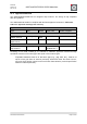
Board thickness of 1.55 mm
Copper layer thickness of 35 µm
Top and bottom solder
9.8. RF Design for deRFsamR21E-23S20
For deRFsamR21E-23S20 two options for the RF signal are available: using the coaxial u.FL
connector to connect an external antenna or if needed in the application, custom designed
RF circuitry using the RF-out pad.
Note: Please get in contact with dresden elektronik to advise for a custom FCC certified
design. If necessary dresden elektronik can provide RF part design data. This may
require signing a Non-Disclosure Agreement.
When designing RF traces on the base board a line impedance of 50 Ω shall be used.
Depending on the base board layer stack construction a microstrip or grounded coplanar
microstrip design can be implemented.
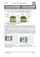
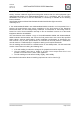
9.8.1. External front end and antenna diversity
The radio module deRFsamR21E-23S20 can be used with an external front end, including
power amplifier (PA) for transmission and low noise amplifier (LNA) for receiving, and
antenna diversity. Figure 11-8 shows a possible design as block diagram. A custom design
can contain a single PA or single LNA or a complete integrated front-end chip. It depends
mainly on the application. Furthermore, it is possible to include a RF switch for driving the
antenna diversity feature. An example block diagram is shown in Figure 11-8.
Figure 11-8: block diagram for external PA/LNA and antenna diversity control
The DIG1 to DIG4 signals of the transceiver are connected internally to the microcontroller
and have to be muxed on ports PA08, PA09, PA14 and PA15. DIG1 to DIG4 can be
activated as alternate pin output functions FECTRL[0..5] by the microcontroller. Please refer
to chapter 33 of ATSAMR21 datasheet [1].
Unbalanced RF output
The radio module deRFsamR21E-23S20 has a 50 Ω unbalanced RF output. For designs
with external RF power amplifier a RF switch is required to separate the TX and RX path.