
User Manual


datasheet
Version 0.9
2017-09-13
deRFsamR21E-23S00/-23S20 datasheet
www.dresden-elektronik.de
Page 22 of 36
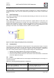
(-) no separate VCC plane usable
(+) separate VCC plane usable
(+) cheaper than 4 layers
(-) more expensive than 2 layers
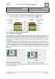
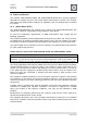
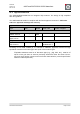
9.5. Traces below the module
Signal traces should not be placed directly below the module to avoid short circuits:
Traces on top layer are not allowed under the module (see Figure 11-2)
Traces on mid layers and bottom layers are allowed (see Figure 11-2)
Figure 11-2: Layer design of 2 and 4 layer boards
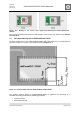
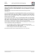
9.6. Placement on the PCB
The PCB design of the radio module base board and placement affects the radio pattern. For
the deRFsamR21E-23S20 with coaxial u.FL connector usage, module placement is not
critical, since the radiating part is placed external to the module and can therefore be placed
everywhere on the board. If the RF-Pad is used, the placement shall be chosen for proper
RF design.
For deRFsamR21E-23S00 with integrated antenna the performance is strongly influenced by
the base board design. The module shall be placed at the edge of the base board. The chip
antenna has to be placed next to the edge as shown in the figures below. The antenna
design is optimized for use on 1.5 mm FR4 PCB baseboard. Best performance is obtained
with the module placed at the corner of the PCB with as much ground plane on the board as
possible.
Figure 11-3: Placing at the edge
Figure 11-4: Placing at the centre edge
Do not place the chip antenna radio module within the base board. This will cause a very
poor radio performance.
Top
Bottom
Mid 1
Mid 2
2 Layer 4 Layer
Module
4 Layer
Traces under
module:
Not allowed
allowed
allowed
allowed
Traces under
module:
Not allowed
allowed