
User Manual


datasheet
Version 0.9
2017-09-13
deRFsamR21E-23S00/-23S20 datasheet
www.dresden-elektronik.de
Page 20 of 36
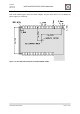
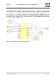
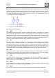
8.3. I2C (TWI)
The I2C (Inter-Integrated Circuit, also referred to as TWI – two wire interface) is a common
interface for sensor connection and it is able to connect several devices at one bus. There is
one clock signal (SCL) and a data signal (SDA). It is necessary to place pull-up resistors for
both lines externally to the radio module for proper function. We recommend the use of
4.7 kΩ resistors as shown in Figure 10-3.
Figure 10-3: Two Wire Interface
8.4. USB
The USB (Universal Serial Bus) interface complies with USB 2.1 specification. It supports
both device and embedded host modes. PA24 (USBDM) and PA25 (USBDP) are routed as
differential lines from the MCU to the radio module side contacts to pins 11 and 12. The
module power supply cannot be operated directly from a 5 V USB source. The module base
board has to implement the required voltage regulator for recommended voltage supply of
3.3 V. For USB operation a minimum supply voltage of 3.0 V is required.
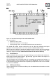
8.5. SPI
The SPI (Serial Peripheral Interface) is a synchronous serial communication interface
commonly used in embedded systems. The SPI Interface on this module is used by the
onboard serial data flash. To add another device to the SPI Bus SCLK, MISO and MOSI can
be used, only another chip select signal (SS) is needed for each device. Any GPIO can be
used for this purpose, except pin 9 (PA18) since it is connected to the chip select of the
onboard data flash. In this example pin 18 (PA28) is used for the SPI Sensor chip select.
8.6. ADC
The module contains an ADC (Analog to Digital Converter) with 12-bit resolution. It supports
sample rates up to 350 ksps. Pin 23 and 24 (PA07 and PA06) are used in this configuration.
The internal reference voltage can be set to 1.0 V, VCC/1.48 and VCC/2.
8.7. SWD
The SWD interface consists of clock signal (SWCLK) and data signal (SWDIO) as well as the
RESET signal for programming and debugging the microcontroller. More details on
programming can be found in Section 12.
8.8. GPIO
In this example pin 17 (PA27) and pin 18 (PA28) are reserved for GPIO usage, but nearly
every pin can be used as GPIO if not used otherwise.
8.9. Reset
The reset pin is low active and has an internal 10k pull-up resistor to power supply VCC.