
User Manual


datasheet
Version 0.9
2017-09-13
deRFsamR21E-23S00/-23S20 datasheet
www.dresden-elektronik.de
Page 2 of 36
Table of contents
1. General description ......................................................................................................... 1
2. Features .......................................................................................................................... 1
1. Overview ......................................................................................................................... 6
2. Applications ..................................................................................................................... 6
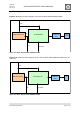
3. Block diagram .................................................................................................................. 7
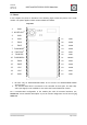
4. Pinout .............................................................................................................................. 9
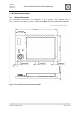
5. Mechanical description .................................................................................................. 10
5.1. Module dimensions............................................................................................... 10
5.2. Recommended footprint ....................................................................................... 11
5.3. ECAD libraries ...................................................................................................... 12
5.4. STEP model library............................................................................................... 12
6. Electrical specification ................................................................................................... 13
6.1. Absolute Maximum Ratings .................................................................................. 13
6.2. Electrical Characteristics ...................................................................................... 13
6.3. TX Power register settings .................................................................................... 14
6.4. Fuse setting .......................................................................................................... 15
7. Onboard SPI Serial Flash .............................................................................................. 16
7.1. Commands ........................................................................................................... 16
7.2. Status register ...................................................................................................... 17
7.3. Flash Timings ....................................................................................................... 17
8. Recommended configuration ......................................................................................... 18
8.1. Signal description ................................................................................................. 19
8.2. UART ................................................................................................................... 19
8.3. I2C (TWI) .............................................................................................................. 20
8.4. USB ...................................................................................................................... 20
8.5. SPI ....................................................................................................................... 20
8.6. ADC ..................................................................................................................... 20
8.7. SWD ..................................................................................................................... 20
8.8. GPIO .................................................................................................................... 20
8.9. Reset .................................................................................................................... 20
9. Application Information .................................................................................................. 21
9.1. PCB Technology .................................................................................................. 21
9.2. Power supply ........................................................................................................ 21
9.3. Ground plane........................................................................................................ 21
9.4. Layers .................................................................................................................. 21
9.5. Traces below the module...................................................................................... 22
9.6. Placement on the PCB ......................................................................................... 22
9.7. Recommended layout for deRFsamR21E-23S00 ................................................. 23
9.8. RF Design for deRFsamR21E-23S20 ................................................................... 24
9.8.1. External front end and antenna diversity ................................................... 24