
User Manual


datasheet
Version 0.9
2017-09-13
deRFsamR21E-23S00/-23S20 datasheet
www.dresden-elektronik.de
Page 17 of 36
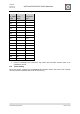
Read Data (up to
30 MHz)
03h
A23-A16
A15-A8
A7-A0
(D7-D0)
(next
byte)
continuous
Fast Read (up to
70 MHz)
0Bh
A23-A16
A15-A8
A7-A0
dummy
(D7-D0)
continuous
Read Manufacturer
and Device ID
9Fh
(M7-M0)
(ID15-
ID8)
(ID7-ID0)
Read ID
90h
dummy
dummy
00h
(M7-M0)
(IRD7-
IRD0)
*make sure not to send a second byte since it may lead to locked and not resettable
protection with some of the flash devices
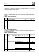
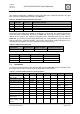
7.2. Status register
The status register is described in Table 9-5.
Table 9-5: flash status register
Bit
content
explanation
Type
S7
SRP
Software Protected
R/W
S6
0
Do not use (always set to 0)
R/W
S5
0
Do not use (always set to 0)
R/W
S4
BP2
Block Protection Bit 2
R/W
S3
BP1
Block Protection Bit 1
R/W
S2
BP0
Block Protection Bit 0
R/W
S1
WEL
Write Enable Latch status
R
S0
BUSY
Indicates ready/busy status
R
Status register bit S5 and S6 always have to be programmed to 0 to ensure proper operation
of the block protection according to Table 9-6. While reading ignore S5 and S6.
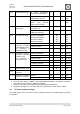
Table 9-6: block protection
BP2
BP1
BP0
Address Range
Portion
0
0
0
None
None
0
0
1
070000h-07FFFFh
Upper 1/8
0
1
0
060000h-07FFFFh
Upper 1/4
0
1
1
040000h-07FFFFh
Upper 1/2
1
X
X
000000h-07FFFFh
All
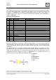
7.3. Flash Timings
Table 9-7 contains typical and maximum values for timings. Typical values refer to the
standard flash AT25SF041 while maximum values apply to all the listed flash devices.
Table 9-7: timings of onboard flash
Parameter
Typ
Max
Unit
Page Program
0.7
2.5
ms
Byte Program
5
us
Block erase 4K
60
300
ms
Block erase 64K
500
2200
ms
Chip Erase
4
10
s
t
CSS
7
ns
t
V
Output Valid
time
8
ns