
User Manual


datasheet
Version 0.9
2017-09-13
deRFsamR21E-23S00/-23S20 datasheet
www.dresden-elektronik.de
Page 13 of 36
6. Electrical specification
This section will outline the main parameters required to build applications. The module
characteristics are determined by the implemented parts. See references at the end of this
document for required datasheet references.
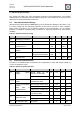
6.1. Absolute Maximum Ratings
Stresses beyond those listed in Table 8-1 may cause permanent damage to the device. This
is a stress rating only and functional operation of the device at these or other conditions
beyond those indicated in the operational sections of this specification are not implied.
Exposure to absolute maximum rating conditions for extended periods may affect device
reliability.
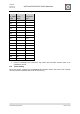
Table 8-1: Absolute maximum ratings
Symbol
Parameter
Condition
Min
Typ
Max
Unit
T
OP
Operating temperature
-40
+85
°C
T
storage
Storage temperature
-40
+125
°C
V
PIN
Pin voltage with respect
to GND and V
CC
GND
-0.3
VCC
+0.3
V
V
CC
Maximum V
CC
pin
voltage
0
3.8
V
V
ESD
ESD robustness
Human Body Model
Charged Device Model
4
550
kV
V
P
RF
Input RF level
+10
dBm
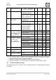
6.2. Electrical Characteristics
The data in the following table is measured at a temperature of 25°C with supply voltage of
3.3 V if not otherwise noted.
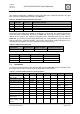
Table 8-2: Electrical specification data
Symbol
Parameter
Condition
Min
Typ
Max
Unit
V
CC
Power supply
voltage
Default Mode for full
operation of data flash
2.5
3.3
3.6
V
For USB interface
3.0
3.3
3.6
V
I
DDOTAU
Current consumption
OTAU
transceiver in RXON state
and data flash write
TBD
mA
I
DD1
Current consumption
of parts
(data flash in
standby mode)
MCU running while(1) loop
3.4
mA
Transceiver in RXON state
11.8
mA
Transceiver in TXON state
13.8
mA
I
DD2
Current consumption
MCU and data flash in
deep power down
5
22
µA
I
DD3
Current consumption
(data flash only)
Read
4
12
mA
Page Program
10
20
P
RF
RF transmit power
conducted
4
dBm