
Specifications

G150XG01
V3 rev 1.0
19/28
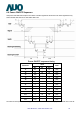
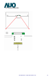
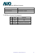
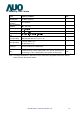
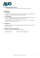
6.6 Power ON/OFF Sequence
VDD power and LED on/off sequence is as below. Interf
ace signals are also shown in the chart. Signals from any
system shall be Hi-Z state or low level when VDD is off.
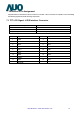
Power ON/OFF sequence timing
Value
Parameter
Min.
Typ. Max.
Units
T1 0.5
- 10 [ms]
T2 30
40 50 [ms]
T3 200
- - [ms]
T4 0.5
- 10 [ms]
T5 10
- - [ms]
T6 10
- - [ms]
T7 0
- - [ms]
T8 10
- - [ms]
T9 -
- 10 [ms]
T10 110
- - [ms]
T11 0
16 50 [ms]
T12 -
- 10 [ms]
T13 1000
- - [ms]
The above on/off sequence should be applied to avoid abnormal function in the display. Please make sure to turn off
Data Modul AG - www.data-modul.com
20