
Specifications

G150XG01
V3 rev 1.0
15/28
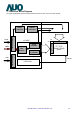
6.3 Signal Description
The module using a pair of LVDS receiver SN75LVDS82(
Texas Instruments) or compatible. LVDS is a differential
signal technology for LCD interface and high speed data transfer device. Transmitter shall be SN75LVDS83(negative
edge sampling) or compatible. The first LVDS port(RxOxxx) transmits odd pixels while the second LVDS port(RxExxx)
transmits even pixels.
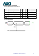
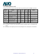
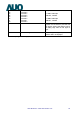
Input Signal Interface
Pin No.
Symbol Description
1 VDD Power Supply, 3.3V (typical)
2 VDD Power Supply, 3.3V (typical)
3 GND Ground
4 REV Reverse Scan [H: Enable; L/NC: Disable]*Note1,3
5 Rin0- - LVDS differential data input
6 Rin0+ + LVDS differential data input
7 GND Ground
8 Rin1- - LVDS differential data input
9 Rin1+ + LVDS differential data input
10 GND Ground
11 Rin2- - LVDS differential data input
12 Rin2+ + LVDS differential data input
13 GND Ground
14 ClkIN- - LVDS differential clock input
15 ClkIN+ + LVDS differential clock input
16 GND Ground
17 Rin3- - LVDS differential data input *Note2
18 Rin3+ - LVDS differential data input *Note2
19 NC/GND Reserved for AUO internal test. Please set it as NC
or Ground.
20 SEL68 Selection for 6 bits/8bits LVDS data input[H/NC: 6bi
ts, L: 8bits]*Note1,3
Note 1: Input signals shall be in low status when VDD is off.
Note 2: For 6bits input mode, pin 17 and pin 18 mus
t be floated.
Note 3: High stands for “3.3V”, Low stands for “0V”, NC stands for “No Connection”.
Data Modul AG - www.data-modul.com
16