Specification G150XG01 V3 incl. Touch - 4W Content: Mechanical Drawing Appendix A: Specification of TFT G150XG01 V3 Appendix B: Specification of Touch AST-150C080A ( Please be aware that some of the values e.g. optical, mechanical etc. of the complete unit (assembled display plus touch panel) might differ from the original values of the individual components.
1 2 4 3 6 5 7 8 A A 328 ±0,3 ODT 309 VAT 305 AAT 304,10 AAD 14,74 (max. 15,53) 326,50 ±0,5 ODD B D E 228,10 AAD 229 AAT 233 VAT 252 ±0,3 ODT 0,75 ±0,5 80 ±1 NOT TO BE DISCLOSED TO THIRD PARTY WITHOUT PERMISSION FROM C CONRAC GMBH / Data Modul AG Contact 253,50 ±0,5 ODD B C 1,25 ±0,5 1 ODD ODT VAT AAT AAD 3 D Outline Dimension Display Outline Dimension Touch Viewing Area Touch Active Area Touch Active Area Display This drawing is only schematic representation of the structure.
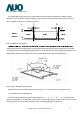
( ) Preliminary Specifications ( v ) Final Specifications Module 15 Inch Color TFT-LCD Model Name G150XG01 V3 Customer Date Approved by Vito Huang Checked & Approved by Date 2010/11/16 Prepared by KuoKang Tseng Note: This Specification is subject to change without notice. 2010/11/16 Audio-Video Business Unit / AU Optronics corporation G150XG01 V3 rev 1.0 Data Modul AG - www.data-modul.
Contents 1. Operating Precautions.....................................................................................4 2. General Description .........................................................................................5 2.1 Display Characteristics...........................................................................................................5 2.2 Optical Characteristics ...........................................................................................................6 3.
Record of Revision Version and Date Rev1.0 2010/11/16 Page Old description First Edition New Description G150XG01 V3 rev 1.0 Data Modul AG - www.data-modul.
1. Operating Precautions 1) Since front polarizer is easily damaged, please be cautious and not to scratch it. 2) Be sure to turn off power supply when inserting or disconnecting from input connector. 3) Wipe off water drop immediately. Long contact with water may cause discoloration or spots. 4) When the panel surface is soiled, wipe it with absorbent cotton or soft cloth. 5) Since the panel is made of glass, it may be broken or cracked if dropped or bumped on hard surface.
2. General Description G150XG01 V3 is a Color Active Matrix Liquid Crystal Display composed of a TFT-LCD display, a driver circuit, and a backlight system. The screen format is intended to support XGA (1024(H) x 768(V)) screen and 16.2M (RGB 8-bits) or 262k colors (RGB 6-bits). All input signals are LVDS interface compatible. All design rules of this module can correspond to PSWG standard. G150XG01 V3 is designed for industrial display applications. 2.
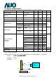
vengdistac 1 with50cm 2.2 Optical Characteristics The optical characteristics are measured under stable conditions at 25 Item Unit Conditions [cd/m2] 100% Dimming White Luminance (center point) Uniformity Contrast Ratio Cross talk Response Time Viewing Angle % 9 Points % [msec] [msec] [msec] Rising Falling Raising + Falling 1 75 80 - 1, 2, 3 400 700 - 4 - 5.7 - 8 1.2 - 2.3 1.5 70 80 - [degree] [degree] Vertical CR = 10 (Upper) (Lower) 50 60 - 0.577 0.627 0.677 0.
Note 2: Definition of 9 points position (Display active area : 304.128(H) x 228.
eurntofcasri#10,thescrn,ovea180°hrizontlad180° Viewngalsthm Note 6: Definition of response time: The output signals of photo detector are measured when the input signals are changed from “White” to “Black” (falling time) and from “Black” to “White” (rising time), respectively. The response time interval is between 10% and 90% of amplitudes. Please refer to the figure as below.
3. Functional Block Diagram The following diagram shows the functional block of the 15 inch color TFT/LCD module: DC/DC Converter AU ASIC Timing Controller Receiver LED Connector + 12V RSDS Transmitter D1 Y-Driver IC LVDS G1 Gate Driver IC LVDS LVDS Connector + 3.3V Gamma Correction Source Driver IC TFT-LCD 1024(2)*768(2) Pixels LED B/L LED Driver G150XG01 V3 rev 1.0 Data Modul AG - www.data-modul.
Bulbshode397anocdestin. 4. Absolute Maximum Ratings 4.1 Absolute Ratings of TFT LCD Module Item Logic/LCD Drive Voltage Symbol Vin Min - 0.3 Max Unit +3.6 [Volt] Max Unit 4.2 Absolute Ratings of Environment Item Operating Temperature Symbol TOP Operation Humidity HOP Storage Humidity HST Storage Temperature Note: Maximum Wet- TST Min -30 8 -30 8 +85 [ C] o 90 [%RH] 90 [%RH] +85 [oC] G150XG01 V3 rev 1.0 Data Modul AG - www.data-modul.
5. Electrical Characteristics 5.1 TFT LCD Module 5.1.1 Power Specification Symbol Parameter Min Typ Max Units 3.0 3.3 3.6 [Volt] VDD Logic/LCD Drive Voltage IDD VDD Current - 700 840 [mA] Irush LCD Inrush Current - - 3 [A] PDD VDD Power - 2.31 2.77 [Watt] Remark ±10% 64 Gray Bar Pattern (VDD=3.3V, at 60Hz) Note 1 64 Gray Bar Pattern (VDD=3.3V, at 60Hz) Note 1: Measurement condition: +3.3V D6 D5 D2 D1 Q3 AO6402 R2 2 S C3 R2 1 Q3 AO6402 G +12.
5.1.2 Signal Electrical Characteristics Input signals shall be low or Hi-Z state when VDD is off. Symbol Item Min. Typ. Max. Unit Remark VTH Differential Input High Threshold - - 100 [mV] VCM=1.2V VTL Differential Input Low Threshold 100 - - [mV] VCM=1.2V Input Differential Voltage 100 400 600 [mV] Differential Input Common Mode Voltage 1.15 1.2 1.45 [V] |VID| VICM VTH/VTL=±100mV Note: LVDS Signal Waveform. G150XG01 V3 rev 1.0 Data Modul AG - www.data-modul.
5.2 Backlight Unit 5.2.1 Parameter guideline for LED Following characteristics are measured under stable condition using a LED driving board at 25 Symbol Parameter Min Typ Max Unit Vcc Input Voltage 10.8 12 12.6 Volt Ivcc Input Curent - 0.61 - A PLED Power Consumption - 7.32 10 Watt FPWM PWM Dimming Frequency 200 - 20k Hz Swing Voltage 4.5 5 5.5 5 - 100 2.0 5 5.
6. Signal Characteristic 6.1 Pixel Format Image Following figure shows the relationship between input signal and LCD pixel format. 6.2 Scanning Direction The following figures show the image seen from the front view. The arrow indicates the direction of scan. AUO AUO Fig. 1 Normal scan (Pin4, REV = Low or NC) Fig. 2 Reverse scan (Pin4, REV = High) G150XG01 V3 rev 1.0 Data Modul AG - www.data-modul.
6.3 Signal Description The module using a pair of LVDS receiver SN75LVDS82(Texas Instruments) or compatible. LVDS is a differential signal technology for LCD interface and high speed data transfer device. Transmitter shall be SN75LVDS83(negative edge sampling) or compatible. The first LVDS port(RxOxxx) transmits odd pixels while the second LVDS port(RxExxx) transmits even pixels. Input Signal Interface Pin No. 1 2 3 4 5 6 7 8 9 Symbol Description VDD Power Supply, 3.
6.4 The Input Data Format 6.4.
B7 B6 B5 B4 B3 B2 B1 B0 RxCLKIN Blue Data 7 Blue Data 6 Blue Data 5 Blue Data 4 Blue Data 3 Blue Data 2 Blue Data 1 Blue Data 0 LVDS Data Clock DE Data Enable Signal Blue-pixel Data For 6Bits LVDS input MSB: B5 ; LSB: B0 For 8Bits LVDS input MSB: B7 ; LSB: B0 The typical frequency is 65MHz. The signal is used to strobe the pixel data and DE signals. All pixel data shall be valid at the falling edge when the DE signal is high. When the signal is high, the pixel data shall be valid to be displayed.
6.5 Interface Timing 6.5.1 Timing Characteristics Signal Clock Timing Vsync Timing Hsync Timing Parameter Symbol Clock frequency 1/ TClock Vertical Section Horizontal Section Period TV Active TVD Blanking TVB Period TH Active THD Blanking THB Frame Rate F Min. 50 Typ. 65 Max. 80 776 806 1023 - 768 - 8 38 255 1074 1344 2047 - 1024 - 50 320 1023 50 60 75 Unit MHz TLine TClock Hz Note: DE mode only. Note : Typical value refer to VESA STANDARD 6.5.
6.6 Power ON/OFF Sequence VDD power and LED on/off sequence is as below. Interface signals are also shown in the chart. Signals from any system shall be Hi-Z state or low level when VDD is off. Power ON/OFF sequence timing Parameter T1 T2 Value Min. Typ. Max. 30 40 50 0.5 - 10 - - 0.
the power when you plug the cable into the input connector or pull the cable out of the connector. G150XG01 V3 rev 1.0 Data Modul AG - www.data-modul.
7. Connector & Pin Assignment Physical interface is described as for the connector on module. These connectors are capable of accommodating the following signals and will be following components. 7.
7.1.1 Connector Illustration SEL68 G150XG01 V3 rev 1.0 Data Modul AG - www.data-modul.
7.2 LED Backlight Unit: LED Driver Connector Connector Name / Designation LED Connector Manufacturer E&T or compatible Connector Model Number 3808K-F05N-02R or compatible Mating Connector Model Number H208K-P05N-02B or compatible 7.3 LED Driver Connector Pin Assignment Pin# Symbol Signal Name 2 GND GND 1 3 4 5 Vcc Enable Dimming NC 12V 5V-On / 0V-Off PWM Dimming or Analog Dimming NC G150XG01 V3 rev 1.0 Data Modul AG - www.data-modul.
/0,3m B hoinur6s0,1cyles 8. Reliability Test Criteria Items Temperature Humidity Bias High Temperature Operation Low Temperature Operation Hot Storage Cold Storage Thermal Shock Test Shock Test (Non-Operating) Required Condition 50 80%,300 hours 85 ,300 hours -3 ,300 hours 85 -3 -2 50G,20ms,Half-sine wave,( ±X, ±Y, ±Z) Vibration Test (Non-Operating) 1.
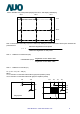
9.1 LCM Outline Dimension (Front View) 9. Mechanical Characteristics Data Modul AG - www.data-modul.com 26 25/28 G150XG01 V3 rev 1.
9.2 LCM Outline Dimension (Rear View) Data Modul AG - www.data-modul.com 27 26/28 G150XG01 V3 rev 1.
10. Label and Packaging 10.1 Shipping Label (on the rear side of TFT-LCD display) V.3 10.2 Carton Package Max capacity: 12pcs TFT-LCD module per carton Max weight: 20 kg per carton Outside dimension of carton: 375(L)mm* 430(W)mm* 353(H)mm G150XG01 V3 rev 1.0 Data Modul AG - www.data-modul.
11 Safety 11.1 Sharp Edge Requirements There will be no sharp edges or comers on the display assembly that could cause injury. 11.2 Materials 11.2.1 Toxicity There will be no carcinogenic materials used anywhere in the display module. If toxic materials are used, they will be reviewed and approved by the responsible AUO toxicologist. 11.2.
Specification AST/ATP Series Revision 11 Version March 23, 2010 Data Modul AG - www.data-modul.
Table of Contents 1. Product Specifications ...........................................................................................................................3 1-1. Product Applicable .............................................................................................................................3 1-2. Structure.............................................................................................................................................3 1-3. Environmental Specifications .
1. Product Specifications 1-1. Product Applicable § This specification is applied to the analog resistive touchscreen: ATP/AST Series. 1-2. Structure § Dimensions, structure, and shape are referred on the drawing attached. 1-3. Environmental Specifications Specification Value Operating Temperature -20°C to 70°C (no condensation) Operating Humidity -20°C to 60°C Less than 90%RH (no condensation) 3 Exceeding 60°C 133.
1-6. Appearance § Scratch, dust (W = width, L = length, D = average diameter = (longest + shortest) /2) Item Width (mm) Length (mm) Acceptable Numbers Linear(Scratch/Dust) Over 0.1mm in diameter refer to the Circular. 0.1≥W>0.05 4≥L 1pcs in φ30mm 0.05≥W>0.03 10≥L 2pcs in φ20mm 0.03≥W 20≥L Acceptable Circular (Scratch/Dust) 0.4≥D>0.3 *1 1pcs in viewing area *1 0.3≥D>0.2 2pcs in φ30mm 0.2≥D Acceptable Total Within 5pcs /panel Applied only in the Active Area.
2. Testing Regulation 2-1. Testing Regulation § If the regulation is not specified, the test is performed under the supplier’s regulation. § Tests are performed under the room temperature unless specified. The room temperature is referred as follows: Temperature: 20°C±5°C Humidity: 65%±10%RH 2-2. Environmental Specifications § Chemical Resistance Test Condition: Tested after leaving the chemical on the surface for 12 hours being wiped off by cloth. Judgement: Must be no effect in appearance. 2-3.
2-4. Electrical Characteristics § Terminal Resistance Test Condition: Top and bottom electrodes are measured at the terminal. Judgement: Must satisfy the specification. § Insulation Resistance Test Neighboring Terminals: Measured by applying the reference voltage to the terminals Active Area Electrodes: Measured by applying the reference voltage to the top and bottom electrodes. Judgement: Must satisfy the specification. 2-5. Appearance § Appearance Test Condition: Tested by an examiner with over 1.
3. Reliability Condition 3-1. Temperature Condition § Temperature Condition Test Following test are performed in the condition with no dew condensation: Cold Test: Tested after leaving the parts in -40°C±3°C for 240 hours and in the room temperature for 2 hours. Heat Test: Tested after leaving the parts in 80°C±3°C for 240 hours and in the room temperature for 2 hours.
5. Handling Notes 5-1. Precautions § This product is intended for use in standard applications (computers, office automation, and other office equipment, industrial, communications, and measurement equipment, personal and household devices, etc.
5-5. Mounting Notes Bezel Bezel edge must be positioned in the area between the Active Area and the Viewing Area. The bezel may press the touchscreen and cause input if the edge enters the Active Area. § Gap between the Bezel and Touchscreen Active Area Viewing Area Bezel Top Electrode A gap of approximately 0.5mm is needed between the bezel and the top electrode. It may cause unexpected input if the gap is too narrow. 0.
6. Warranty 6-1. Warranty Period § The warranty period is limited to 1 year from the date of shipping. The warranty for the initial defection such as appearance defection is limited to 1 month. § Any defected parts under proper use will be examined by the supplier and replaced by the new parts if the defection is considered to be caused by the supplier. § The replacement is subject to be included in the next lot. 6-2.
7. Revision history Rev1 (April 15, 1998) Initial release Rev2 (June 1, 1999) The overall revision by specification review. Rev3 (April 1, 2002) The address in the office was changed by the move. Rev4 (August 16, 2002) 1-4.Activation Force is changed “50g± 30g” to “0.5N±0.3”. 1-4.Light Transmission is changed 76% to 80%(TYP). Rev5 (September 3, 2002) 1-3.Operating Temperature is changed “0°C to 60°C” to “-20°C to 70°C”. 1-3.Storing Temperature is changed “-20°C to 70°C” to “-40°C to 80°C” 1-4.
Rev10 (November 10, 2006) The specification item name was changed. 1-3.”Storing Temperature” to “Storage Temperature” 1-3.”Storing Humidity” to “Storage Humidity” 1-4.”Operating Load” to “Activation Force” 1-4.”Light Transmissivity” to “Light Transmittance” 1-4.”Top Surface Hardness” to “Surface Hardness” 2-3.”Operating Load Test” to “Activation Force Test” 2-3.”Operating Load” to “Activation Force” 3-1.”Operationg Load” to “Activation Force” 1-4.Operating Force is changed “0.5N±0.3N” to “0.05N to 0.8N”.
DI SPLAYS AND EMBEDDED SOLUTIONS DI SPLAYS AND EMBEDDED SOLUTIONS DATA MODUL Headquarters Munich Landsberger Str. 322 D-80687 Munich - Germany Phone: +49-89-56017-0 Fax: +49-89-56017-119 www.data-modul.com Sales Office Hamburg Borsteler Chaussee 51 D-22453 Hamburg - Germany Phone: +49-40-42947377-0 Sales Office Duesseldorf Fritz-Vomfelde-Str. 8 D-40547 Duesseldorf - Germany Phone: +49-211-52709-0 Sales Office Scandinavia Lundsmindevej 5 DK-6000 Kolding - Denmark Phone: +45-75-224477 DATA MODUL France, S.