
Specifications

PRODUCT SPECIFICATION
Version 2.4 23 August 2011 18 / 28
The copyright belongs to CHIMEI InnoLux. Any unauthorized use is prohibited.
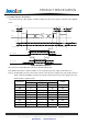
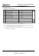
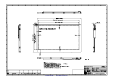
6.3 POWER ON/OFF SEQUENCE
To prevent a latch-up or DC operation of LCD assembly, the power on/off sequence should be as the diagram
below
LVDS
VCC
Vi
10%
90%
T2
T1
T3
0.1VCC
0.9VCC
0.9VCC
0.1VCC
T4
VALID
T7
0.9Vi
0.9Vi
0.1Vi
0.1Vi
PWM DIMMING
T9
10%
90%
T8
BL ON/OFF
T5
10%
90%
T6
Power ON/OFF sequence
Note (1) Please avoid floating state of interface signal at invalid period.
Note (2) When the interface signal is invalid, be sure to pull down the power supply of LCD VCC to 0 V.
Note (3) The Backlight converter power must be turned on after the power supply for the logic and the interface
signal is valid. The Backlight converter power must be turned off before the power supply for the logic
and the interface signal is invalid.
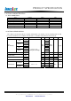
Value
Parameter
Min Typ Max
Units
T1 0.5
-
10 ms
T2 0
-
50 ms
T3 0
-
50 ms
T4 500
- -
ms
T5 20
- -
ms
T6 10
- -
ms
T7 5
300 ms
T8 10
- -
ms
T9 10
- -
ms
Data Modul AG - www.data-modul.com