
Specifications

PRODUCT SPECIFICATION
Version 2.4 23 August 2011 12 / 28
The copyright belongs to CHIMEI InnoLux. Any unauthorized use is prohibited.
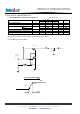
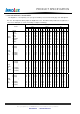
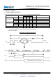
5. INPUT TERMINAL PIN ASSIGNMENT
5.1 LVDS I/O PIN ASSIGNMENT
Pin Name I/O Description
1 RX3+ I
2 RX3- I
LVDS differential data input Pair 3.
3 NC I No Connected
4 FRC I
Dithering control setting
When FRC=H, the width of data input 8 bits
When FRC=L, the width of data input 6 bits and set Dx0 and Dx1 to logical low
(Default pull low)
5 GND I Ground
6 RXC+ I
7 RXC- I
LVDS differential Clock input Pair
8 GND I Ground
9 RX2+ I
10 RX2- I
LVDS differential data input Pair 2
11 GND I Ground
12 RX1+ I
13 RX1- I
LVDS differential data input Pair 1
14 GND I Ground
15 RX0+ I
16 RX0- I
LVDS differential data input Pair 0
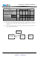
17 LR I
Shift direction of Source Driver IC internal shift register is controlled by this pin as
show below:
LR=H SO1Æ ……SO1200 (Default pull high)
LR=L SO1200Æ…….SO1
18 UD I
Gate Driver Up/down scan setting
When UD=H, reverse scan
When UD=L, normal scan (Default pull low)
19 VCC_IN I Digital power supply (+3.3V)
20 VCC_IN I Digital power supply (+3.3V)
Note (1) User’s connector Part No.: 076B20-0048RA-G4,Starconn or equivalent
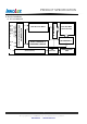
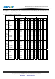
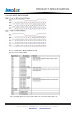
5.2 BACKLIGHT PIN ASSIGNMENT (Converter connector pin)
No Symbol I/O Description
1 Vi
I Converter input voltage
2 ADJ I Backlight Adjust
3 EN I Enable pin
4 V
GND
Converter ground
Note (1) User’s connector Part No: LM123S004HTF13,4 PIN,UNE
Data Modul AG - www.data-modul.com