
User manual
DLP-USB245M User Manual
Copyright © DLP Design 2002 Page 6 of 15
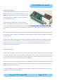
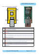
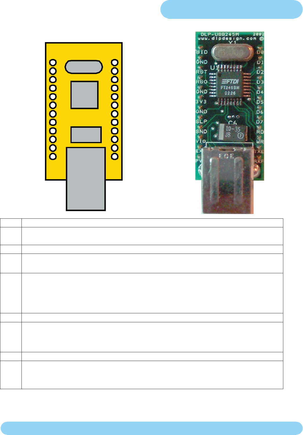
Table 1 - DLP-USB245M PINOUT DESCRIPTION
Pin# Description
1 BOARD ID (Out) Identies the board as either a DLP-USB245M or DLP-USB232M. High for DLP-
USB232M and low for DLP-USB245M.
2 Ground
3 RESET# (In) Can be used by an external device to reset the FT245BM. If not required this pin must
be tied to VCC.
4 RESETO# (Out) Output of the internal Reset Generator. Stays high impedance for ~ 2ms after
VCC > 3.5v and the internal clock starts up, then clamps it’s output to the 3.3v output of the internal
regulator. Taking RESET# low will also force RSTOUT# to go high impedance. RSTOUT# is NOT
affected by a USB Bus Reset.
5 Ground
6 3V3OUT (Out) Output from the integrated L.D.O. regulator. It’s primary purpose is to provide the
internal 3.3v supply to the USB transceiver cell and the RSTOUT# pin. A small amount of current
(<= 5mA ) can be drawn from this pin to power external 3.3v logic if required.
7 Ground
8 SLEEP (Out) Goes Low after the device is congured via USB, then high during USB suspend.
Can be used to control power to external logic using a P-Channel Logic Level
MOSFET switch.
1
12 13
24