
Datasheet


DEM 20485 SYH-LY Product Specification
Version: 3 PAGE: 4
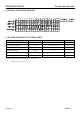
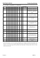
5. PIN ASSIGNMENT
Pin No. Symbol
Function
1 VSS Ground terminal of module
2 VDD Supply terminal of module +5 V
3 V0 Power Supply for Liquid crystal Drive
4 RS Register Select, RS = 0 (Instruction Register), RS = 1 (Data Register)
5 R/W Read / Write, R/W = 1 (Read), R/W = 0 (Write)
6 E Enable
7 DB0
Bi-directional Data Bus, Data Transfer is performed
once , thru DB0~DB7 , in
the case of interface data . Length is 8-
bits; and twice , thru DB4~DB7 in the
case of interface data length is 4-bits.
Upper four bits first then lower four
bits .
8 DB1
9 DB2
10 DB3
11 DB4
12 DB5
13 DB6
14 DB7
15 K
B00
Please also refer to 6.1 PCB drawing and description.
16 A
15 A
B01
16 K