
Datasheet


DEM 16227 SYH-LY Product Specification
VERSION: 2 PAGE: 19
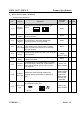
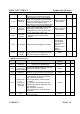
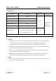
6.5 PCB/COB
No. Defects Description
Acceptance
standard
MAJ MIN
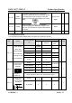
6.5.1
Improper
Epoxy
Cover
l Contacts exposure within
the white circle for COB chip
bonding.
l The height of epoxy cover is
out of the product
specifications and drawing.
l The epoxy cover over the
COB chip exceeds the circle
by more than 2mm in
diameter, which is the
maximum distance the
epoxy cover is allowed to
exceed the circle.
l Existence of obvious linear
mark(s) or chip-exposing
pinhole on the epoxy cover.
l The pinhole diameter on the
epoxy over exceeds
0.25mm and there is foreign
matter in the pinhole.
Reject √
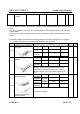
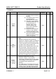
6.5.2
PCB
appearance
defect
1. Oxidized or contaminated gold fingers on
PCB.
2. Bubbles on PCB after reflow-soldering.
3. Exposure of conductive copper foil caused by
peeled off or scratched solder-resist coating.
For the conductive area of PCB repaired with
the solder resist coating material, the
diameter ψ of the repaired area on the circuit
must not exceed 1.3mm while for the non-
conductive area of PCB repaired with the
solder resist coating material, the diameter ψ
must not exceed 2.6mm; the total number of
repaired areas on PCB must be less than 10;
otherwise, the PCB must be rejected.
Reject √
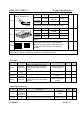
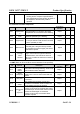
6.5.3
Wrong or
missing
Component
s on PCB
1) Components on PCB are not the same as
defined by drawing such as wrong,
excessive, missing, or mis-polarized
components. (The bias circuit of LCD voltage
or the backlight current limiting resistance is
not adjusted unless specified by the
customer.)
2) The JUMP short on PCB shall conform to the
mechanical drawing. If excessive or missing
soldering occurs, the PCB shall be rejected.
3
) For components particularly required by the
Reject √