
Datasheet


DEM 16227 SYH-LY Product Specification
VERSION: 2 PAGE: 15
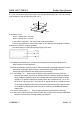
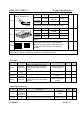
6.1.10
Pattern
distortion
The pattern displayed
width
is
either
wider
,
narrower or
deformed
than
the
specified,
caused
by its
misalignment and resulting
in
unwanted
heave(s)
or
missing:|Ia-Ib|≤1/4W(W
is the
normal
width
)
|Ia-Ib|>1/4W,
Reject
√
6.1.11
Voltage
When normally
working
the
bias
between
measured
voltage
and
designed
voltage is
more
than ±4% (if
at or below
5V, inspect
at
the
tolerance
of
+/-0.2V)
Reject
√
6.1.12
High current
The current of LCD is higher than the standard one.
Reject
√
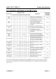
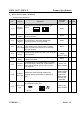
6.2 LCD appearance defect:
6.2.1 Dot and line defects (defined within VA, spots out of VA do not account)
NO. Items
Average diameter
(d)
Acceptable quantity
MAJ
MIN
VA≤600mm
2
600mm2<VA≤5
000mm2
5000mm2
<VA≤20000
mm2
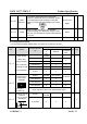
6.2.1.1
Spot
defects
(black
spot,
foreign
material,
nick,
scratches,
including
LC
with
wrong
orientation)
d≤0.10
Not
counted
Not counted
Not counted
√
0.10<d≤0.20 3 3
4
0.20<d≤0.25 0 1
0.25<d≤0.30 0 0 1
0.30<d≤0.40 0 0 0
0.40<d 0 0 0
6.2.1.2
Line defects
(scratches and
linear foreign
materials)
Line length=L
Line width=W
W≤0.01
Not
counted
Not counted
Not counted
√
L≤2.0,W≤0.02 2 3
L≤3.0,W≤0.03 1 2 3
L≤3.0,W≤0.05 0 1 2
Note: when W>0.1mm it can regard as spot defect.
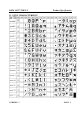
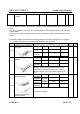
6.2.1.3
Polarizer with air
bubble or
convex-concave
dots defect
W
d≤0.15
Not
counted
Not counted
Not counted
√
0.15<d≤0.3 2 3 3