
Datasheet


DEM 16217 SYH-LY-CYR22 Product Specification
Version: 3 PAGE: 4
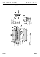
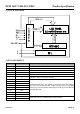
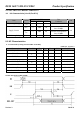
4. BLOCK DIAGRAM
VSS
VDD
V0
RS
R/ W
E
DB 0
~
DB 7
ST7066U-0T
COM1~16
L CD PANEL
2Li neX16Char act er s
SEG0~40
SEG41~8
0
ST7065C
B/ L
A
K
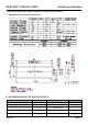
5. PIN ASSIGNMENT
Pin No. Symbol
Function
1 VSS Ground terminal of module.
2 VDD Supply terminal of module 5.0V
3 V0 Power Supply for liquid crystal drive
4 RS Register select RS=0: Instruction register; Rs=1: Data register
5 R/W Read or Write Select Signal
6 E Read/Write R/W=1: Read; R/W=0: Write
7 DB0
8 DB1
9 DB2
10 DB3
11 DB4
12 DB5
13 DB6
14 DB7
Bi-directional data bus, data transfer is performed once, thru DB0 to
DB7, in the case of interface data. Length is 8-bits; and twice, thru DB4
to DB7 in the case of interface data length is 4-bits. Upper four bits first
then lower four bits.
15 L-(K)
16 L+(A)
Please also refer to 6.1 PCB drawing and description.