
Datasheet


DEM 16210 SGH (FPCR) Product Specification
Version:5 PAGE: 3
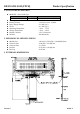
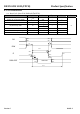
4. BLOCK DIAGRAM
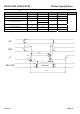
5. PIN DESCRIPTION
Pin No. Name I/O Description
1 VSS P
GND: 0V
2 V5 P
Power supply for LCD driver
3 VDD P
VDD: +5V
4 RS I
Register select signal
0: instruction register (write), Busy flag, address counter (read)
1: Data register (write, read)
5 R/W I
Read/Write control signal
0:Write 1:Read
6 E I
Read/Write start signal
7 DB0
8 DB1 Lower 4 tri-state bi-directional data bus for transmitting data between MPU
9 DB2 and NT7603. not used during 4-bit operation.
10 DB3
11 DB4
12 DB5 Higher 4 tri-state bi-directional data bus for transmitting data between MPU
13 DB6 and NT7603. DB7 is also used as busy flag.
14 DB7
I/O
6. DISPLAY DATA RAM (DDRAM)
LCD
Controller
NT7603
LCD PANEL
2 x 16 Characters
VSS
V5
VDD
RS
R/W
E
DB0~DB7
COM1~COM16
SEG1~SEG80