
Datasheet


Electrical Characteristics @T
A
= 25°C unless otherwise specified
Characteristic
DS30436 Rev. 8 - 2 2 of 4
www.diodes.com
DMMT5551/DMMT5551S
© Diodes Incorporated
Symbol Min Max Unit Test Condition
OFF CHARACTERISTICS (Note 7)
Collector-Base Breakdown Voltage
V
(BR)CBO
180
⎯
V
I
C
= 100μA, I
E
= 0
Collector-Emitter Breakdown Voltage
V
(BR)CEO
160
⎯
V
I
C
= 1.0mA, I
B
= 0
Emitter-Base Breakdown Voltage
V
(BR)EBO
6.0
⎯
V
I
E
= 10μA, I
C
= 0
Collector Cutoff Current
I
CBO
⎯
50
nA
μA
V
CB
= 120V, I
E
= 0
V
CB
= 120V, I
E
= 0, T
A
= 100°C
Emitter Cutoff Current
I
EBO
⎯
50 nA
V
EB
= 4.0V, I
C
= 0
ON CHARACTERISTICS (Note 7)
DC Current Gain (Note 8)
h
FE
80
80
30
⎯
250
⎯
⎯
I
C
= 1.0mA, V
CE
= 5.0V
I
C
= 10mA, V
CE
= 5.0V
I
C
= 50mA, V
CE
= 5.0V
Collector-Emitter Saturation Voltage
V
CE(SAT)
⎯
0.15
0.20
V
I
C
= 10mA, I
B
= 1.0mA
I
C
= 50mA, I
B
= 5.0mA
Base-Emitter Saturation Voltage
V
BE(SAT)
⎯
1.0 V
I
C
= 10mA, I
B
= 1.0mA
I
C
= 50mA, I
B
= 5.0mA
SMALL SIGNAL CHARACTERISTICS
Output Capacitance
C
obo
⎯
6.0 pF
V
CB
= 10V, f = 1.0MHz, I
E
= 0
Small Signal Current Gain
h
FE
50 250
⎯
V
CE
= 10V, I
C
= 1.0mA,
f = 1.0kHz
Current Gain-Bandwidth Product
f
T
100 300 MHz
V
CE
= 10V, I
C
= 10mA,
f = 100MHz
Noise Figure NF
⎯
8.0 dB
V
CE
= 5.0V, I
C
= 200μA,
R
S
= 1.0kΩ,
f = 1.0kHz
Notes: 7. Short duration pulse test used to minimize self-heating effect.
8. The DC Current Gain, h
FE
, (matched at I
C
= 10mA and V
CE
= 5V) Collector Emitter Saturation Voltage, V
CE(SAT)
, and Base Emitter Saturation Voltage,
V
BE(SAT)
are matched with typical matched tolerances of 1% and maximum of 2%.
0.04
0.05
0.06
0.07
0.08
0.09
0.15
0.14
0.13
0.12
0.11
0.10
110100
1,000
V,
C
O
LLE
C
T
O
R
T
O
EMI
T
T
E
R
SATURATION VOLTAGE (V)
CE(SAT)
I , COLLECTOR CURRENT (mA)
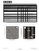
Fig. 2, Collector Emitter Saturation Voltage
vs. Collector Current
C
I
I
C
B
= 10
T = 150°C
A
T = 25°C
A
T = -50°C
A
0
50
100
25 50
75
100 125
150
175
200
P
,
P
O
WE
R
DISSI
P
A
T
I
O
N (mW)
D
T , AMBIENT TEMPERATURE (°C)
Fig. 1, Max Power Dissipation vs.
Ambient Temperature
A
150
200
250
300
350
400
0