
Specifications

AMBE-3000™ Vocoder Chip Users Manual
Version 2.8, August, 2011
Electrical Characteristics and
Requirements
1.8 V
supply voltage should not reach 0.3 V until 3v3 has reached 2.5 V. This ensures the reset signal from the I/O pin has
propagated through the I/O buffer to provide power-on reset to all the modules inside the device.
In other words, 3.3-V and 1.8-V can ramp together.
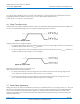
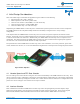
3.6 Signal Transition Levels
Note that some of the signals use different reference voltages, see Table 4 Recommended Operating Conditions. Output levels
are driven to a minimum logic-high level of 2.4 V and to a maximum logic-low level of 0.4 V.
Figure 9 Output Levels
Output transition times are specified as follows:
For a high-to-low transition, the level at which the output is said to be no longer high is below V
OH(MIN)
and the level
at which the output is said to be low is V
OL(MAX)
and lower.
For a low-to-high transition, the level at which the output is said to be no longer low is above V
OL(MAX)
and the level
at which the output is said to be high is V
OH(MIN)
and higher.
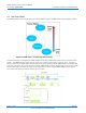
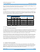
Figure 10 Input Levels
Input levels are as follows 0.8 V (V
IL
) and 2.0 V (V
IH
)
Input transition times are specified as follows:
For a high-to-low transition on an input signal, the level at which the input is said to be no longer high is below
V
IH(Min)
and the level at which the input is said to be low is V
IL(Max)
and lower.
For a low-to-high transition on an input signal, the level at which the input is said to be no longer low is above
V
IL(Max)
and the level at which the input is said to be high is V
IH(Min)
and higher.
3.7 Power-Down Sequencing:
During power-down, the device reset should be asserted low (8 μs, minimum) before the 1.8 V supply reaches 1.5 V. This will
help to keep on-chip flash logic in reset prior to the 3v3and 1.8 V power supplies ramping down. It is recommended that the
device reset control from “Low-Dropout (LDO)” regulators or voltage supervisors be used to meet this constraint. LDO
regulators that facilitate power-sequencing (with the aid of additional external components) may be used to meet the power
sequencing requirement.
(Subject to Change) Page 22
DVSI CONFIDENTIAL PROPRIETARY