
User`s manual

AMBE-2000™ Vocoder Chip
User’s Manual Version 4.9
DVSI Confidential Proprietary, Subject to Change Page 21
Visit us at www.dvsinc.com
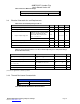
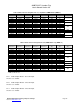
Table 3-D Absolute Maximum Ratings
Absolute Maximum Ratings
Voltage Range on any Pin with Respect to Ground -0.3V to 4.6V
3.9 Electrical Characteristics and Requirements
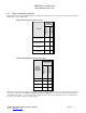
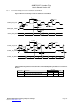
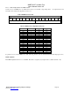
Table 3-E Recommended Operating Conditions
Parameter Min Nom Max Unit
DV
DD
Device Supply Voltage 3 3.3 3.6 V
V
SS
Supply Voltage, GND - 0 - V
RESETN (pin 69), CLOCK_MODE
(pin 51), X2/CLKIN (pin 68),
pins 44,45,46,47,48,52,53,54
DV
DD
= 3.3 ±0.3 V
2.5
V
IH
High-level input voltage, I/O
All other inputs
2.0
- DV
DD
+ 0.3
V
V
IL
Low-level input voltage -0.3 - 0.8 V
I
OH
High-level output current - - -300
µA
I
OL
Low-level output current - - 1.5 mA
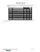
Table 3-F Electrical Characteristics over Recommended Operating Case Temperature Range
(Unless Otherwise Noted)
Parameter Test Conditions
MIN TYP† MAX
Unit
V
OH
High-level output voltage‡ V
DD
= 3.3 ±V, I
OH
= MAX
2.4 V
V
OL
Low-level output voltage‡
I
OL
= MAX 0.4 V
I
I
Input current in high impedance
(V
I
= V
SS
to V
DD
)
V
DD
= MAX, V
I
= V
SS
to V
DD
-10 10
µA
C
I
Input capacitance
10 pF
C
O
Output capacitance
10 pF
† All values are typical unless otherwise specified.
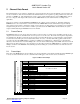
3.10 Thermal Resistance Characteristics
Thermal Resistance Characteristics
R
ΘJA
58 °C/W
R
ΘJC
10 °C/W
Table 3G Thermal Resistance Characteristics