
User`s manual

AMBE-2000™ Vocoder Chip
User’s Manual Version 4.9
DVSI Confidential Proprietary, Subject to Change Page 16
Visit us at www.dvsinc.com
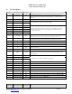
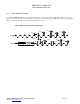
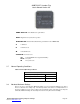
Table 3-A X2/CLKIN and CLKOUT Timing Parameters
Reference Parameter Min Max Units
t
c
(CI)
Cycle time, X2/CLKIN Integer PLL multiplier N (N=4) 20 400 ns
t
f
(CL)
Fall time, X2/CLKIN
4 ns
t
r
(CL)
Rise time, X2/CLKIN
4 ns
t
w
(CIL)
Pulse duration, X2/CLKIN low 6
ns
t
w
(CIH)
Pulse duration, X2/CLKIN high 6
ns
t
p
Transitory phase, PLL lock-up time
50
µs
t
c
(CO)
Cycle time, CLKOUT (typical is
t
c
(CI)/4
15
ns
t
d
(CIH-CO)
Delay time, X2/CLKIN high/low to CLKOUT high/low 4 16 ns
t
f
(CO)/t
r
(CO)
Fall/Rise time, CLKOUT (typical is 2 ns)
t
w
(COL)
Pulse duration, CLKOUT low H-4 H ns
t
w
(COH)
Pulse duration, CLKOUT high H-4 H ns
• CLKOUT is shown for reference only. It is not to be connected in the circuit.
• H = 7.629 ns
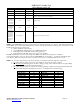
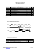
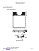
Figure 3-B Hardware Reset Timing Diagram
Table 3-B Reset Timing Parameters
Reference Parameter Min Max Units
t
h
(RS)
Hold time, RS after CLKOUT low 0
ns
t
w
(RSL)
Pulse duration, RS low 50
µs
t
su
(RS)
Setup time, RS before X2/CLKIN low 5
ns
t
su
(INT)
Setup time, INTn, NMI, RS before CLKOUT low 10
ns
• CLKOUT is shown for reference only. It should not be connected in the circuit.
t
w
(RSL)
t
su
(RS)
t
h
(RS)
t
su
(INT)
~
~
~
~
~
~
X2/CLKIN
RESETN
CLKOUT