
User`s manual

AMBE-2000™ Vocoder Chip
User’s Manual Version 4.9
DVSI Confidential Proprietary, Subject to Change Page 14
Visit us at www.dvsinc.com
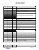
41 CODEC_TX_DATA Output PCM Data from AMBE-2000™ to D/A Converter
27 CODEC_RX_CLK Input A/D Serial clock. Should be connected to CODEC_TX_CLK
33 CODEC_TX_CLK Input D/A Serial clock Should be connected to CODEC_RX_CLK
51 CLOCK_MODE Input
If high enables crystal oscillator option for clock source. If low then external oscillator
option is selected. See Section 3.5 for details.
8,11,12,23
36,39,44,45
46, 47,48
49,54,57,64
76,87,90
V
DD
Power Supply Voltage
1,9,10,25,26
35,40,50,52
53,56,63,65
88,89
GND Power Ground
2,3,4,5,6,7,
13,14,15,16
17,18,19,21
22,24,43,55
58,59,60,61
62,66,91,92
93,94,95,96
97,98,99
100
No Connection These pins must remain unconnected
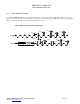
NOTE 1: The AMBE-2000™ expects an encoder packet to be read approximately every 20 msec. Following the initial reset,
wait for EPR to go low and read the initial packet (t
0
). 20 msec later, the next packet (t
1
) should be ready. For packet t
1
and all
following packets use the procedure below:
1) Wait for slightly less than 20 msec.
2) Assert CHAN_TX_STB and read word on CHAN_TX_DATA.
3) If transmitted word not 0x13EC, discard it and repeat step 2.
4) If transmitted word 0x13EC, read 23 more words (rest of packet).
The EPR signal should not be used as an interrupt. The EPR is only valid for the first high to low transition.
A new packet should be ready every 20 msec after the initial EPR high to low transition. A packet read should take place
every 20 msec. If there is a delay in the read (i.e. a packet is missed), it is recommended that the device be reset.
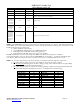
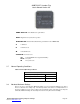
NOTE 2: To prevent possible damage to the chip be sure that your circuit meets the following three requirements.
1) No signals should be applied to the device (this includes clocks) before the power is applied.
2) The clock and reset must be applied to the device during power up. If the clock and reset are not applied during
power up, high currents may flow damaging the device.
3) All of the configuration I/O pins of the device should be pulled up or pulled down through individual 10 K ohm
resistors to limit current flow through the I/O sections. See Table below for the affected pins.
Descriptive Name Pin Number Descriptive Name Pin Number
CHAN_SEL1 77 VAD_EN 86
CHAN_SEL0 75 ECHOCAN_EN 78
CODEC_SEL1 85 SLEEP_EN 83
CODEC_SEL0 84 SLIP_EN 82
RATE_SEL4 74 SPFT_EN 79
RATE_SEL3 73 BAUD_SEL0 80
RATE_SEL2 72 BAUD_SEL1 81
RATE_SEL1 71
RATE_SEL0 70