
User's Guide

HE863 Family Hardware User Guide
1vv0300891 Rev.5
- 2011-03-18
Reproduction forbidden without Telit Communications S.p.A’s. written authorization - All Rights
Reserved. Page 80 of 89
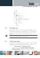
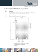
Placement of microvias not covered by solder resist is not
recommended, unless the microvia carries the same signal of the
pad itself.
Holes in pad are allowed only for blind holes and not for
through holes.
Recommendations for PCB pad surfaces:
The PCB must be able to resist the higher temperatures, which
are occurring at the lead-free process. This issue should be
discussed with the PCB-supplier. Generally, the wet-ability of
tin-lead solder paste on the described surface plating is
better compared to lead-free solder paste.
14.1.5. Solder paste