
User's Guide

HE863 Family Hardware User Guide
1vv0300891 Rev.5
- 2011-03-18
Reproduction forbidden without Telit Communications S.p.A’s. written authorization - All Rights
Reserved. Page 79 of 89
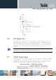
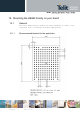
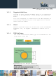
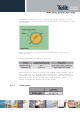
14.1.2. Suggested Inhibit Area
In order to easily rework the HE863 Family it is suggested to
consider on the application a 1.5mm Inhibit area around the
module.
It is also suggested, as common rule for an SMT component, to
avoid having a mechanical part of the application in direct
contact with the module.
14.1.3. Stencil
Stencil’s apertures layout can be the same of the recommended
footprint (1:1), we suggest a thickness of stencil foil ≥
120µm.
14.1.4. PCB Pad Design
“Non solder mask defined” (NSMD) type is recommended for the
solder pads on the PCB.
Recommendations for PCB pad dimensions