
User's Guide

HE863 Family Hardware User Guide
1vv0300891 Rev.5
- 2011-03-18
Reproduction forbidden without Telit Communications S.p.A’s. written authorization - All Rights
Reserved. Page 51 of 89
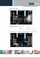
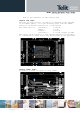
Layer5, inner layer:
Same cut-out with layer 6’s should be applied to match 50ohm.
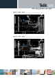
Layer6, Bottom layer:
The trace info as; Thickness = 0.035 mm
Width = 1.2 mm
Length = 18.42 mm
Clearance = 2.0 mm (Signal to GND)
The actual trace limits in a host system should be calculated
to correspond to 50 ohm which may be provided by the pcb maker.