
User's Guide

HE863 Family Hardware User Guide
1vv0300891 Rev.5
- 2011-03-18
Reproduction forbidden without Telit Communications S.p.A’s. written authorization - All Rights
Reserved. Page 44 of 89
2W max during class12 GPRS upload. This generated heat will
be mostly conducted to the ground plane under the HE863
Family; you must ensure that your application can dissipate
heat.
In the WCDMA/HSPA mode, since HE863 Family emits RF signals
continuously during transmission, you must pay special
attention how to dissipate the heat generated.
The current consumption will be up to about 710mA in HSPA
continuously at the maximum TX output power (23dBm). Thus, you
must arrange the PCB area as large as possible under HE863
Family which you will mount.
You must mount HE863 Family on the large ground area of your
application board and make many ground vias to dissipate the
heat.
The peak current consumption in the GSM mode is higher than
that in WCDMA. However, considering the heat sink is more
important in case of WCDMA.
As mentioned before, a GSM signal is bursty, thus, the
temperature drift is more insensible than WCDMA. Consequently,
if you prescribe the heat dissipation in the WCDMA mode, you
don’t need to think more about the GSM mode.
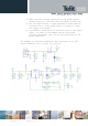
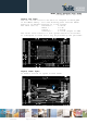
6.2.3. Power Supply PCB Layout Guidelines
As seen in the electrical design guidelines, the power supply
must have a low ESR capacitor on the output to cut the current
peaks and a protection diode on the input to protect the
supply from spikes and polarity inversion. The placement of
these components is crucial for the correct working of the
circuitry. A misplaced component can be useless or can even
decrease the power supply performances.
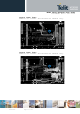
The Bypass low ESR capacitor must be placed close to
the Telit HE863 Family power input pads, or in the
case the power supply is a switching type, it can be
placed close to the inductor to cut the ripple if the
PCB trace from the capacitor to HE863 Family is wide
enough to ensure a drop-less connection even during
the 2A current peaks.
The protection diode must be placed close to the input
connector where the power source is drained.
The PCB traces from the input connector to the power
regulator. IC must be wide enough to ensure no voltage
drops to occur when the 2A current peaks are absorbed.