
User manual

Kontron Compact Computers AG SMX945 Detailed Manual V1.1
59
7.4. USB2 Signal
Use the following general routing and placement guidelines when laying out a new design. These guidelines
will help to minimize signal quality and EMI problems. The USB 2.0 validation efforts focused on a four-layer
motherboard where the first layer is a signal layer, the second plane is power, the third plane is ground and
the fourth is a signal layer. This results in the placement of most of the routing on the fourth plane (closest to
the ground plane), allowing a higher component density on the first plane.
1. Place the ICH7-M and major components on the un-routed board first. With minimum trace lengths,
route high-speed clock, periodic signals, and USB 2.0 differential pairs first. Maintain maximum
possible distance between high-speed clocks/periodic signals to USB 2.0 differential pairs and any
connector leaving the PCB (i.e., I/O connectors, control and signal headers, or power connectors).
2. USB 2.0 signals should be ground referenced.
3. Route USB 2.0 signals using a minimum of vias and corners.
4. When it becomes necessary to turn 90°, use two 45° turns or an arc instead of making a single 90°
turn. This reduces reflections on the signal by minimizing impedance discontinuities.
5. Do not route USB 2.0 traces under crystals, oscillators, clock synthesizers, magnetic devices or ICs
that use and/or duplicate clocks.
6. Stubs on high speed USB signals should be avoided, as stubs will cause signal reflections and affect
signal quality. If a stub is unavoidable in the design, the sum of all stubs for a particular line should
not be greater than 200 mils.
7. Route all traces over continuous planes (VCC or GND), with no interruptions. If at all possible, avoid
crossing over anti-etch.
8. Separate signal traces into similar categories and route similar signal traces together (such as
routing differential pairs together).
9. Keep USB 2.0 USB signals clear of the core logic set. High current transients are produced during
internal state transitions and can be very difficult to filter out.
10. Place a 10uF/10V tantalum capacitor and a 100nF capacitor directly at the power pin of each USB2
connector.
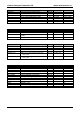
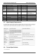
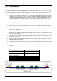
USB Signals:
Signal Group USB2
Topology Differential
Referred plane Ground
Impedance 90 Ohm +/-15%
Trace with / pair spacing 4mil / 4.5mil
Number of allowed vias 2
Maximal length 20cm
Length matching +/- 0.5mm
Remarks: -