
User manual

Kontron Compact Computers AG SMX945 Detailed Manual V1.1
56
7. DESIGN RULES FOR THE INTEGRATION
On this product, there are many very fast interfaces. Some of these interfaces work differentially and must be
routed in twisted pair with equal flight times. All power signals must be designed as power planes including
all decoupling capacitors. The power planes and their vias must be capable of transporting the maximum
energy.
7.1. Video Signals
The DAC channel (red, green, blue) outputs should be routed as single-ended shielded routes. An analog
switch should be used in order to provide the proper termination that is required for high-performance video
signal integrity. The analog switch should exhibit a low “on” resistance (< 8) and low parasitic capacitance
(<10 pF). The output routing from the analog switch should be routed as single-ended 37.5- impedance to
the 75- termination resistors that are located near the VGA connector on the motherboard and the VGA
connector on the docking station. The single- ended routing after these 75- termination resistors to the pi-
filter and then to the VGA connector should ideally be 75.
HSYNC and VSYNC signals are connected to the analog display attached to the VGA connector. These are
3.3-V outputs from the GMCH. A 39 Ohm series resistor is required before routing to the VGA connector.
Also, capacitors (28 pF - 33 pF) before and after the series resistor may be needed to meet the VESA
rise/fall time specification.
Unidirectional buffers (high impedance buffers) are required on both HSYNC and VSYNC to prevent
potential electrical overstress and illegal operation of the GMCH, since some display monitors may attempt
to drive HSYNC and VSYNC signals back to GMCH.
DDCADATA and DDCACLK are 3.3-V IO buffers connecting the GMCH to the monitor. If higher signaling
voltage (5 V) is required by the monitor, level shifting devices may be used. Pull-up resistors of 2.2-k (or the
appropriate value derived from simulation) are required on each of these signals.
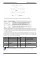
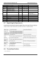
LVDS Signals:
Signal Group LVDS
Topology Differential
Referred plane Ground
Impedance 100 Ohm +/-15%
Trace with / pair spacing 4mil / 7mil
Number of allowed vias 2
Maximal length 20cm
Length matching +/- 1mm
Remarks: -
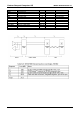
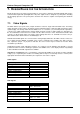
DVO Signals:
Signal Group DVO
Topology Data: single
Clocks: differential
Referred plane Ground
Impedance 55 Ohm +/-15%
Trace with / pair spacing 4mil / 8mil
Number of allowed vias 2
Maximal length 10cm
Clock length matching Data: +/- 10mm
Clocks: +/- 1mm
Remarks: -