
User manual

Kontron Compact Computers AG SMX945 Detailed Manual V1.1
51
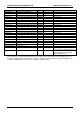
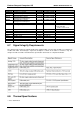
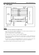
Signal Description I/O Termination Remarks
PCIE0_RX+ PCI Express channel 0
PCIE0_RX- Receive Input differential pair I PCIE Spec. 1.0A
PCIE0_TX+ PCI Express channel 0
PCIE0_TX- Transmit Output differential pair O PCIE Spec. 1.0A
PCIE1_RX+ PCI Express channel 1
PCIE1_RX- Receive Input differential pair I PCIE Spec. 1.0A
PCIE1_TX+ PCI Express channel 1
PCIE1_TX- Transmit Output differential pair O PCIE Spec. 1.0A
PCIE2_RX+ PCI Express channel 2
PCIE2_RX- Receive Input differential pair I PCIE Spec. 1.0A
PCIE2_TX+ PCI Express channel 2
PCIE2_TX- Transmit Output differential pair O PCIE Spec. 1.0A
PCIE3_RX+ PCI Express channel 3
PCIE3_RX- Receive Input differential pair I PCIE Spec. 1.0A
PCIE3_TX+ PCI Express channel 3
PCIE3_TX- Transmit Output differential pair O PCIE Spec. 1.0A
PCIE_CLK_REF+ PCI Express Reference Clock 0 PCIE PD 50Ohm Spec 1.0a
PCIE_CLK_REF- or Lanes 0 to 3
PCE_WAKE# PCI Express Wake Event I 3.3VSB
PU 1K 3.3VSB
Sideband wake signal asserted
by components requesting wakeup
PCIE_Reset# Reset# O 3.3V Generated from the PCI_Reset#,
coming from Pin C23, buffered
with a 74HC08 (3.3V).
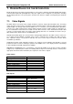
The insertion losses previously allowed for the slot card and slot card connector are re-allocated for use on
the carrier board, allowing longer carrier board trace lengths and more carrier board design flexibility. The
module and COM Express™ connector-loss budgets remain the same.