
User manual


Kontron Compact Computers AG SMX945 Detailed Manual V1.1
47
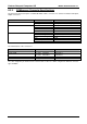
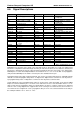
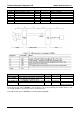
6.6. Signal Descriptions
Signal Description I/O Termination Remarks
VCC Power Supply +5VDC ±5% P External supply for external
peripheral
GND Power Ground P External supply
3.3V Power Supply +3.3VDC P External supply for external
peripheral
NC Not Connected N.A. Do not connect
SERIRQ Serial Interrupt request I 3.3V PU 10K 3.3V
PCICLK1-4 Clock output O 3.3V
REQ0-3# Bus request I 3.3V PU 8k2 3.3V REQ1-3# is a boot strap signal,
5V Tolerant
GNT0-3# Bus grant O 3.3V GNT2/3# is a boot strap signal
AD0-31 Address/Data bus lines I/O 3.3V 5V Tolerant
CBE0-3# Bus command/byte enables I/O 3.3V 5V Tolerant
PAR Bus parity I/O 3.3V 5V Tolerant
SERR# Bus system error I/O 3.3V PU 8k2 3.3V 5V Tolerant
PERR# Bus grant parity error I/O 3.3V PU 8k2 3.3V 5V Tolerant
PME# Bus power management
event
I/O 3.3VSB PU 8k2 3.3V SB
LOCK# Bus lock I/O 3.3V PU 8k2 3.3V 5V Tolerant
DEVSEL# Bus device select I/O 3.3V PU 8k2 3.3V 5V Tolerant
TRDY# Bus target ready I/O 3.3V PU 8k2 3.3V 5V Tolerant
IRDY# Bus initiator ready I/O 3.3V PU 8k2 3.3V 5V Tolerant
STOP# Bus stop I/O 3.3V PU 8k2 3.3V 5V Tolerant
FRAME# Bus frame I/O 3.3V PU 8k2 3.3V 5V Tolerant
PCIRST# Bus reset O 3.3V Asserted during system reset
INTA# Bus interrupt A I 3.3V PU 8k2 3.3V 5V Tolerant
INTB# Bus interrupt B I 3.3V PU 8k2 3.3V 5V Tolerant
INTC# Bus interrupt C I 3.3V PU 8k2 3.3V 5V Tolerant
INTD# Bus interrupt D I 3.3V PU 8k2 3.3V 5V Tolerant
PCI_Reset# Bus Reset# O 3.3V Generated out of Pin C23
with a 74HC08 buffer (3.3V)
COM Express™ specifies only a single copy of the PCI clock for off-module use. If only one carrier board
PCI device is implemented, then that single clock may be routed to the device. If more than one carrier board
PCI device is implemented, then the carrier board should replicate the PCI clock using a zero delay buffer.
COM Express™ carrier board implementations should allow 1.6 ns +/- 0.1 ns for the PCI clock propagation
delay from the COM Express™ module connector pin to the destination device pin.
Propagation delay varies with construction details such as trace geometry, PCB stack up, and PCB material
dielectric constant. Propagation delay values of 140ps/inch to 180ps/inch are common for outer layer traces.
A propagation delay value of 180ps/inch is common for inner layer traces/carrier boards.
Using 180ps/inch as the propagation delay value for an inner layer carrier board PCI clock, then the COM
Express™ carrier board delay of 1.6 ns works out to 8.88 inches of trace. If the destination device is on an
add-on card, then the propagation delay associated with the 2.5 inches of add-on card trace are deducted
from the 1.6 ns. Using 160ps/inch as a typical value for an outer layer slot card clock trace, the 2.5 inches of
slot card clock trace length work out to a propagation delay of 0.4 ns. The carrier board PCI clock delay in
this example would be 1.6 ns - 0.4 ns or 1.2 ns.