
User manual


DIGITAL-LOGIC AG MSM800SEV/SEL/BEV/XEV/XEL Detailed Manual V1.5
74
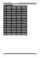
X110 LPC-Port
Only for factory and POD-Diagnostic use.
Pin Signal Pin Signal
1 VCC 3.3V 2 LAD0
3 LFrame# 4 LAD1
5 PCI_RST# 6 LAD2
7 FWH_TBL# 8 LAD3
9 VCC 5V 10 PCI_RST#
11 LPC_Clock 12 FWH_Control
13 Ground 14 NC
X230 JTAG-Port
Pin Signal Pin Signal
1 TCK 2 TMS
3 TDI 4 TDO
7. JUMPER LOCATIONS ON THE BOARD
The following figure shows the location of all jumper blocks on the MSB800/L board. The numbers shown in
this figure are silk screened on the board so that the pins can easily be located. This chapter refers to the
individual pins for these jumpers. The default jumper settings are indicated with asterisks.
Be careful: some jumpers are soldering bridges; you will need a miniature soldering station with a vacuum
pump.
7.1. The Jumpers on MSM800SEV V2.1
Settings written in bold are defaults!
Jumper Structure 1-2 / open 2-3 / closed Remarks
J1
Compact Flash select
Slave
Master Top
J2
Power On Switch Push button
always on
Top
J7
a)
CMOS/EEPROM reset
Normal function
Reset
R163
LCD VDD 5V
3.3V
Top
R164
LCD VDD
3.3V
5V Top
R165
LCD BKL (Backlight)
12V
b)
5V Bottom
R166
LCD BKL (Backlight) 5V
12V
b)
Bottom
a) For the MSM800BEV/XEV/XEL – refer to Section 4.7.3 for important information!
b) The 12V will not be generated on the board, you must supply the 12V from an external PSU through
connector X1 pin4.
Attention!
Never install R163 and R164 or R165 and R166 together!
The board will be destroyed!