
Specifications


DUAL
ASYNCHRONOUS
RECEIVER/TRANSMITTER
(DUART)
SCN2681
SERIES
CTUR and CTLR - Counter/Timer
Registers
The CTUA and
CTlA
hold the eight MSBs
and eight LSBs respectively
of
the value
to
be used by the
counter/timer
In
either the
counter
or
timer
modes
of
operation. The
minimum
value which may be loaded Into
the CTUA/CTLA registers is 0002,6' Note
that these registers are
.....
rite·only and can·
not
be read
by
the CPU.
In the
timer
(programmable divider) mode,
the
CIT generates a square wave with a
period
of
twice
the value (in
clock
periods)
of
the CTUA and
CTlA.
If the value
in.
CTUA
or
CTlA
is changed, the current
half·period will not be affected, but subse·
quent half periods will be. In
this
mode the
CiT runs continuously. Aeceipt of a start
counter
command (read
with
A3-AO =
1110)
causes the
counter
to
terminate the
ABSOLUTE MAXIMUM RATINGS'
PARAMETER
Operating ambient temperature
2
Storage temperature
All voltages with respect to ground
3
NOTES.
current
timing
cycle and to begin a new
cycle using the values in CTUA and
CTlA.
The counter ready
status
bit (ISA[3)) is set
once each
cycle
of
the square wave. The
bit is reset by a stop
counter
command
(read
with
A3-AO = 1111). The command,
however, does not stop the
CIT. The gen·
erated square wave
is
output
on OP3
if
it
is
programmed to be the
CIT output.
In the counter mode, the CIT counts
down
the number
of
pulses
loaded into CTUA
and
CTlA
by the CPU. Counting begins
upon receipt
of
a start
counter
command.
Upon
reaChing terminal
count
(0000,6), the
counter ready interrupt
bit
(ISA[3J)
is set.
The counter
continues
counting
past the
terminal
count
until
stopped by the CPU. If
OP3
is programmed
to
be the
output
of
the
CIT,
the
output
remains high
until
terminal
count is reached, at which time
it
goes
low. The
output
returns
to
the high state
RATING
UNIT
o
to
+
70
·C
-
65
to
+
150
·C
-0.5
to +
6.0
V
,
Suesses
aDo.e
l~ose
"Slea
·Jnaer ADsol"le MaXimum RatIngs may
cause
permanent
damage
to
tha
.:leVice.
Th,S
'5
a
stress
r.l.~t;l
Only
and
lur.ct!Qnal
operallon
01
lne
devIce
.t
tnese
or ill any
other
conditIon
aDove thOSe
.nd"ated
In
tne
~perat.on
section
01
t".s
spec.I,.;atlon
.,
not .mpl,ed
2 For
cperat.ng
ilt ele-olted
'emperatules.
t~e
cev'ce
must
be
Clerateo
based
on +
150'C
max.mum
junclton
lemperature
3.
TI'IIS
;lloduct
."Cluces
CtlCL;.tt'f
spec",cally
aeslgned
lor
the
protect,on
ol,ts
,Mernal Clev,ces
'rom
damag,nt;l
el.
I$cts
01
eacess.-e
sta!.c
challfe.
Nenethe'ess
.•
,
.$
suggested
Ihat
convent,onal
precaullons
De
talc
en
10
avo,d ap·
p'y.ng
any v:"talOes arlfer
than
:he
'ated
max.ma
DC
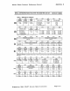
ELECTRICAL CHARACTERISTICS
TA
= o·c to + 70·C, Vee=
50V
:!: 5%45.6
PARAMETER
TEST CONDITIONS
Min
V
IL
Input low voltage
V
IH
Input
high voltage (except
Xl/ClK)
2.0
V
iH
Input high voltage
(Xl/ClK)
4.0
VOL.
Output
low voltage
I
IOL= 2.4mA
I
V
OH
Output
htgh voltage (except o.c. outputs)
IOH= -
400j4A
2.4
and ISA[3] is cleared when the
counter
is
stopped by a
stop
counter command. The
CPU may change the
values
of
CTUA and
CTlA
at any time,
but
the new
count
be-
comes effective only on the next start
counter command.
If
new values have not
been
loaded, the previous
count
values
are
preserved and used for the next count
cycle.
In
the
counter
mode, the current value of
the upper and
lower 8
bits
of
the counter
(CTU,
CTl)
may be read by the
CPU.
It
IS
recommended that the
counter
be stop·
ped when reading
to
prevent potential
;>ro·
blems which may
occur
if
a carry from the
lower 8·bits
to
the upper a·bits occurs bet·
ween the times that both halves
of
the
counter
are read. However.
nole
that a
subsequent
start
counter
command will
cause the
counter
to
begin a new count
cycle using the values in CTUA and
CTlA.
LIMITS
UNIT
Typ Max
0.8
V
I
V
V
i
0.4
V
V
IlL
Input leakage current
VIN=OtOV
cc
-10
10
j4A
ILL
Data bus 3·state leakage current
Vo:
0
to
Vcc
-10
10
/loA
lac
Open
collector
output
leakage current
I
Vo=OtoV
cc
-10
10
/loA
Icc
Power
supply current
150
mA
NOTES:
4.
Paramala"
.ra
.aud
o.ar
specll'eCl
lemper.ture
'linga.
5.
All
1011ige
m.aluram.nll
are
r,r,rencld
10
ground
IGNO).
For
IlIt,ng.
Iii ,f\pul
"gnlll
,
..
ing
bll
....
n 0.4V
.nd
2.4V
..
'11'1.
"anll.,on
I,m.
0120'1'
m&ll,mum
AlIl,me
mauur.·
m.nll
are
ref"anced
II
'nput
vOI!.gll
01
a 8'.'
.nd
2.0V
.nd
oulpul
.oltlg
..
01
0.8V
and
2.0V
...
pprop"llI.
8.
T~p.c:al
••
1
....
Ire
II
+
25'C,
lyplCl'
,upply
vOl
"011.
Ind
lyPlCl1 proc
..
"ng
p.r.mlt
....