
Specifications


Multi
Sleve
Product
Reference
Manual
Appendlx
H
DUAL
ASYNCHRONOUS
RECEIVER/TRANSMITTER
(DUART)
SCN2681
SERIES
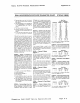
PIN DESIGNATION (Continued)
APPLICABLE
MNEMONIC
TYPE NAME
AND
FUNCTION
I
40
28
24
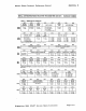
IP4 X
I
Input
4:
General
purpose
input.
or
channel A receiver external
clock
Input
(RxCAI
Whe:'\
thl!
external
clock
is
used
by
the
receiver. the received data is sampled on
the
riSing
edge
of
the
clocl<.
IP5
X I
Input
5:
General
purpose
input.
or
channel
B
transmitter
external
clock
input
(TxCBI
When
the
.,"mal
clock
Is
us.c
.,
the
"an,m'tte'.
the
"an,mllted
data"
Clockee on the Iailinol
edge
of
the
clock.
1P6
X
I
Input
6:
General
purpose
input
cr
channel B receiver external
clock
input
iRxCB).
When
the
I
external
clock
IS
used by
the
r~celver.
the received
data
is sampled on
the
riSing edg''!
of
tho,:
clock.
Vee
X X X I
Power
Supply:
-+
5V
supply
input
GND
X X X I
Ground
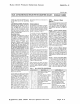
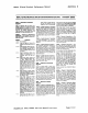
BLOCK DIAGRAM
The
2681
DUART
consists
of
the
following
eight
major
sections:
data
bus
butler.
operation
contrOl.
interrupt
control.
tim·
ing.
communications
channels
A and
B.
in·
put
port
and
output
port. Refer
to
the
blOCk.
diagram.
Data Bus Buffer
The
data
bus
buffer
provides
the
interface
between
the
external
and
internal
data
busses.
It
is
controlled
by
the
operation
control
block
to
allow
read and
write
operations
to
take
place
between
the
con-
trolling
CPU ana
the
DUART.
Operation Control
The
operation
control
logic
receives
operation
commands
from
the
CPU and
generates
a~propriate
signals
to
internal
sections
to
control
eevice
operation.
It
conta;ns
address
decoding
and
reac
and
write
circuits
to
permit
communlcalio~s
WI~rl
the
microprocessor
via
the
data
bus
buffer.
Interrupt Control
A
single
active
low
interrUPt outPl.lt
(INTRN)
is
provided
which
is
activated
upon
the
occurence
01
any
of
eight
inter-
nai events_
Associated
with
the
intern;pt
system
are
the
interrupt
mask
register
(IMR) and
the
interrupt
stat~s
register
(lSR). The IMR may
be-
programmed
to
select
O:'l!y
certai"
coneitions
to
cause
INTRN
to
be assertE'd. The ISR can be reae
by
the
CPU
to
determine
aa
curre"II)'
ac·
tlve
interrupting
conditions
Outputs
OP3-0P7
can be
programme:
to
provide
discrete
interrupt
output~
for
the
transmitter~.
receivers. and
counte.'tloner
-
Timing Circuits
The
timing
block
ccnSlsts
of
a
crystal
oscillator.
a baud rate
~enerator.
a pro-
grammable
16-t·it cOl.lnter/tlmer. and
fou~
Clock
selectors.
The
crystal
oscillator
operates
directl)'
from
a 3.6864MHz crys·
tal
connected
across
tne X1/CLK and
X2
inputs.
If
an
extr~nal
cloc"
of
tne
ap~roPrt
ate
frequency
IS
available. it may
Oe
con-
nected
to
X 1!CLK. The
clock
serl/es
as
tne
basic
timing
reference
for
the
baud rate
generator
(BRG).
the
counter'tlmer.
and
otner
internal
CHcl.its. A
clock
signal
within
th~
limits
specified
·n
the
speclflca·
tions
section
of
thiS
do'a
sheet
must
alwa,s
be supplie;d te
the
DUART
The baud rate
generato~
operates
from
the
oscillator
or
e)terna!
clock
inpu!
and
IS
capable
of
generating
18
commonly
used
data
comruunlcatlon5
baud
rates
ranging
from
50 t:. 36.4K baud Tr.e clock
outputs
from
the
BRG are at
1SX
the actual boud
rate. The
counter:tlmel
can be used as a
timer
te
produce
a
16X
Clock for a
r
./
other
bal:C
:ate
by
e('Jun~ing
0o,",,,
tnc
crystal
cloc~
cr
a'1
e,tern;,!
Ci(;C~
Tnt'
fO.Jr
cloe";
select~r~
ailow
tn£:
Indepe-:dent srlectl:->"
for each receiver ana
tran~mltter.
Of any
ot
these
baLia rates or an eY.ternal
tin"ng
~Ig·
nai.
The
counter/timer
(crr:
car;
b~
~rograrr,·
med
to
us€' one
of
several
timing
sources
as
its
inpul
The
output
o'
tne
err
'S
aval;'
able
to
tilE
clock
sele,;tors
a'1J
e.o'.
also
~F.
programmed
to
be outp:.;t at
OP3.
In
tl)~
.
counter
mOde. tne
C0nte~'5
of
the
CfT
CCl"l
be read
by
the
CPJ
anc
it
can
be
stoppe:!
ana
started
under
prograrr
control.
In the
timer
moOe. the CfT
acts
as a program·
mabie
diVide'
Signetics
2681
DUART
Device
Specifications
Communications Channels
A and B
I
Each
commurllcallons
channel
of
tne
2691
comprises
a full
duplex
as)'nchronous
re-
ceiverltransmitter
(UART).
The
operating
frequE'ncy
for
each receiver and
transmit-
ter
ca~
be
selectee
Independe:r'otlr'
from
the
ba.Jd rate {jenerc\!or.
tf'e
ccunter
time~.
or
from
an external
input.
The
transmitter
accepts
paralie!
data
from
the CPU.
converts
It
to
a serla.
bit
stream.
inserts
the
appropriate
start.
5:0P
and
c~·
tlonal
parity
bi:s
and
outtluts
a
com-CS:h!
sena,
stream
oi
data
on
tne
T)r.D
output
pin
ll'le
rece'ver
accepts
serla'
:tata on
th£-
RxD pin. CGr.llens this
se"a
Input
te
paraliel forrr,at.
ct",eci<s
for
sta't
Oit.
stop
bit.
panty
Olt
(If any).
or
brea\(
co~d!tl:~r
a~d
senc~
an assemb!e::; cr-.aracle' to
tne
CPU
Input Port
The Inpl,;ts to
tnls
unlall,h€:;: 7-.,:
~o·t
car.
be
rt:aj
t,y
tnE'
CFU
b,'
pe·f:/rrr"';
arE-a:]
opera'lc:,'"
<.I:
ajd-Is!:
D-f
t..
t:
;~
',;ut
'e·
sl.lt~
.•
1:
i!
;i'f;'('. 1 '"
~'Ii~
...
10""
,r,pl.lt
re5.:I~s
In a iog
c.
0
D·
\III'
alwa,s
be reao a:; a
1:'9"
...
1.
Thf'
f
,·,5
Of
~tllS
P'='f
'
ea"
also
ser
..
L
as
a;JX!!:a~1
Ir:;: .Jts
to
c:cr:a:~
portions
Clf
ttl';'
DUA.r:;.T
10';IC
FOur
chan:Je·ct·sta'~
Oe:e:!CrS
a'e
pr::;
Vldt;:;
....
~.c~.
are
ass0:I"ltl.:l
II"t"
tn~.uts
IF:-. IP2.
IP1.
a;H~
IPC
A
h'g-
..
tr:.·I(,
...
or
10
.....
tu·higt,
tran!..llor.
of
II-leSE;
l"\putS
lasting
!c"QP~
It,aro
2:'-50
•.
5
"",d:
set
the
corre·
sp(;r',dtng
t
..
:
In
the
Ir.;>.;! por" iN
I:
cheong,"
reg 1St£:';
Tt,P
tll~
,H€:
cl:::arp:
",.t'
en It·,,;
reg:ster
I~.
r€"O
D~
tt.~·
CI-ol,:
Ar-.,
cnang£:
o!
~'2te
Gi<n
,,:50
t&
Wugramme:!
t:
generotc
a~\
Intp~rur;'
t(.
the
CF~
Page
H-4