
Specifications


Multi
Slave
Product
Re£erence
Hanual
Appendix
H
I
I
I
I
DUAL
ASYNCHRONOUS
RECEIVER/TRANSMITTER
(DUARn
SCN2681
SERIES
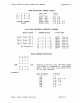
PIN DESIGNATION
MNEMONIC
DO-D7
CEN
WRN
RON
AO-A3
RESET
INTRN
X1'ClK
X2
RlCOA
RxOB
TxOA
Tx08
OPO
OP1
OP2
OP3
OP4
OP5
OPS
OP7
IPO
IP1
IP2
IP3
i
i
I
I
I
i
I
I
APPLICABLE
40
21
24
X
X X
X
X
I
X
X
X
I
X
X X X
X
I
X X
X
X
X
X X
I
)(
X
X
i
X
I
X
X
I
X X X
X X
X
X X x
x X x
I
I
I
I
I
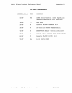
TYPE
1/0
I
I
I
I
I
0
I
0
o
o
o
o
o
o
o
o
o
o
NAME AND FUNCTION
Data
BUI:
Bldirectional3·state
data
bus
used
to
transfer
commands, data and
status
between
the OUART and the CPU.
DO
is the least
significant
bit.
I Chip Enablo: Active
low
Input signal. Wtlen
lOW,
data transfers oetween
the
CPU and the
OUART
are enabled on
00-07
as contrOlled by the WRN, RON and
AO-Al
inputs.
When
high,
I places the
00-07
lines
in the 3·stato
condition.
I
Writ.
Strobo: When
lOW
and CEN
IS
also
lOW,
the
contents
of
the
data
bus
is
loaded
into
the
, addressed register. The transfer
cccurs
on
the
rising
edga
of
tha signal.
I
I
R."d
Strob.:
When low and CEN
IS
also low, causes tha
contants
of
the addrassed
reoister
to
be presented on the I'jata bus, The read
cycle
begins
on
tha
falling edga
of
RON.
I Addr8ac
Inputl:
Sele~t
the
OUART
int~rnal
registers
and
ports
for readJwrite operations.
I
Ruot:
A t-Igh
Ip.vel
clears internal registers (SRA, SRB, IMR,ISR, OPR, OPCR),
putsOPO-OP7
In the high state,
stops
the counterltllT':er, and
puts
cnannp.ls A and B
in
the
inactiva
stata,
INlth
lhe
TxOA and TxOB
outputs
in the m,lIk (high) state.
!
Intorrupt
R~u
••
t:
Active
low, open drain,
output
which
signals
the CPU that one
or
m"re
of
i the eight
maskabl~
Interrupting
conditions
are true.
! Crystal
1:
Crystal
or
external clock input. A
crystal
or
clock
of
the specified
limits
must
be
I suppl!ed .It all times. When a crystal
is
used, a capaCitor
must
be
connected
from thiS
pin
to
I ground (see figure
5).
/CryDtll.2:
Connect.ion for ottler side
of
ttle crystal. Should be conO'lcted to
ground
if
a
Icrystal
IS
not used. When a crystal
IS
used. a
capacitor
must
be connected
from
tttis
pin
to
Iground
(see figure 5).
I
Channel A
Rocolv~r
S.rlol
olt.
Input: The least
significant
bi.
t
is
received first,
'Mark'
IS high,
'space'
is
low. •
i
Chann.'
B Rocolvor Sorlal
Oat.
Input: The least
significant
bit
IS
received
first.
'Mark'
is
high
..
I
'space'
IS
low.
Chann.1 A
Transmltt.,
Sorl.1 Data
Output:
The least
significant
bit
is
transmitted
first. ThiS
output
IS
held 10 the 'mark'
condition
wtlen "",e
transmitter
is
disabled, idle,
or
when operat"
,
109
In local ioopback mode. 'Mark' ,s tllgh,
'space'
IS
low.
I Channol B
Transmltt.r
Ser'.'
Oata
Output:
The least
significant
bit
is
transmitted
first.
This
!
output
is tleld in the 'mark' condit,,)n when the
transmitter
is disabled, Idle,
or
when operat·
ling
in local
100~bacK
mode. 'Mark'
IS
high, ·space'
is
lOIN.
I
Output
0: General purpose
output.
or
channel A request
to
send (RTSAN, active
lOIN).
Can
be
;jeactivated
on receive
or
transmit
:
Output
1:
General puro;)se output.
or
c~al'r.el
B request
to
send (RTSBN. actil;8
reIN).
Can
be
! deactivated on receive
or
transmit.
I
Output
2:
General purpose
output,
or channel A
transmitter
1X
or
t6X
clock
output,
or
chan-
I nel
bo
receiver
IX
clock
output.
i OutPLIt 3: General purpose output, or open dralO. active
low
counterltimer
output,
or
channel
I
B
transmitter
tX
clock
output,
or
channel B receiver
IX
clock
output.
Output
4: General purpose
output,
or channel A open drain, active low, RlCRDYAlFFULLA
out·
I put.
I
~~?ut5:
General purpose
output,
or
channel B open drain, active low, RlCRO'tB/FFULLB
out·
Output
6:
GeMral
purpose output,
or
channel A open drain, active low. TxROYA
output.
Output
7:
General purpose output,
or
Channel B open draIn, active low, TxROYB
output.
Input
0:
General purpose input,
or
channel
A.
clear to send act iva
low
input
iCTSAN).
Input
1:
General purpose input,
or
channel B
clear
to
'lend active
low
Input
(CTSBN,.
Input
2:
General purpose Input,
or
counterllimer
external
clock
input.
Input
3: General purpose IOput,
or
channel A
transmitter
external
clock
input
(TxCA). When
the
external
clock
is
used by the transmitter, the
transmitted
data
is
clocked
on
the
falling
edge
of
the clock.
Signe~ics
2681
DUART
Device
Speci£ications
Page
H-3