
User`s guide


A.2 PCI Sparse I/O Space
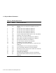
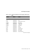
Table A–3 Time-of-Year Clock Device Addresses
Offset
Latched
Index
Physical
Address Register
70 0 85.8000.0E00 Seconds
70 1 85.8000.0E00 Seconds alarm
70 2 85.8000.0E00 Minutes
70 3 85.8000.0E00 Minutes alarm
70 4 85.8000.0E00 Hour
70 5 85.8000.0E00 Hour alarm
70 6 85.8000.0E00 Day of week
70 7 85.8000.0E00 Day of month
70 8 85.8000.0E00 Month
70 9 85.8000.0E00 Year
70 A 85.8000.0E00 Register A
70 B 85.8000.0E00 Register B
70 C 85.8000.0E00 Register C
70 D 85.8000.0E00 Register D
71 — 85.8000.0E20 TOY clock chip select
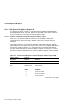
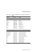
A.2.1.4 Flash ROM Segment Select Register
The flash ROM is partitioned into two 512KB segments. The segments are
selected by flash_adr19. To select the first 512KB segment, write a value of
0 to ISA port address 0x800
16
. To access the second 512KB segment, write a
value of 1 to this register. Alternatively, using the debug monitor, you can type
command wb 800 0 or wb 800 1.
Table A–4 lists the register address for the flash ROM segment select register.
This register is write-only. Refer to Section A.3.1 for dense space flash ROM
memory addresses.
Table A–4 Flash ROM Segment Select Register
Offset Physical Address Register
x800 85.8001.0000 Flash ROM segment select
I/O Space Address Maps A–7