
User`s guide
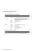

4.2 21164 Address Mapping to PCI Space
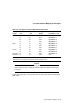
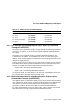
Table 4–11 Hardware-Specific Register Space
CPU Address
<39:28> Selected Region
CPU Address
<27:6>
CPU Address
<5:0>
1000 0111 0100 CIA control, diagnostic, error
registers
LW address 00 0000
1000 0111 0101 CIA memory control registers LW address 00 0000
1000 0111 0110 CIA PCI address translation LW address 00 0000
1000 0111 0111 Reserved — —
1000 0111 1xxx Reserved — —
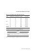
4.2.9 PCI-to-Physical Memory Addressing
Incoming 32-bit or 64-bit PCI memory addresses have to be mapped to
the EB164’s 30-bit physical memory addresses. The EB164 provides four
programmable address windows that control access of PCI peripherals to
system memory. The mapping from the PCI address to the physical address
can be direct (physical mapping, with an extension register) or scatter-gather
mapped (virtual). These four address windows are referred to as the PCI target
windows. The following three registers are associated with each window:
• PCI base register
• PCI mask register
• Translated base register
In addition, there is an extra register associated with window three only.
This is the PCI DAC_BASE register and is used for PCI 64-bit addressing.
However, EB164 only supports up to a maximum of 512MB of main memory.
This precludes any benefit from the CIA chip accepting 64-bit DAC addressing.
Refer to the DECchip 21171 Core Logic Chipset Technical Reference Manual for
more details on DAC addressing (dual address cycle mode).
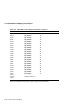
The PCI mask register provides a mask corresponding to bits <31:20> of an
incoming PCI address. The size of each window can be programmed to be from
1MB to 4GB, in powers of two, by masking bits of the incoming PCI address by
using the PCI mask register. This is shown in Table 4–12.
4–20 System Address Mapping