
User`s guide
4.2 21164 Address Mapping to PCI Space
There are two classes of targets for PCI configuration read and write
commands: devices on the primary PCI bus and peripherals on hierarchical
(buffered, secondary) PCI buses, which are accessed through bridge chips.
Address usage during PCI configuration cycles varies depending on the
intended target of the configuration cycle.
Peripherals are selected during a PCI configuration cycle if their initialization
device select (IDSEL) pin is asserted, the PCI bus command indicates
a configuration read or write operation, and address bits <1:0> are 00
(type 0). Address bits <7:2> select a dword (longword) register in the
peripheral’s 256-byte configuration address space. Accesses can use byte
masks. Peripherals that integrate multiple functional units (example: SCSI
and Ethernet) can provide configuration spaces for each function. Address
bits <10:8> can be decoded by the peripheral to select one of eight functional
units. Address bits <31:11> are used to generate IDSEL signals. Typically,
the IDSEL pin of each PCI peripheral is connected to a unique address line.
This requires that only one bit of the field AD<31:11> is asserted in a given
cycle. The EB164 forces zeros on PCI_AD<31:24> during configuration cycles.
Therefore, only PCI_AD<23:11> can be used to drive an IDSEL.
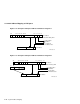
If the PCI cycle is a configuration read or write cycle, but address bits <1:0>
= 01 (type 1), then a device on a hierarchical bus is being selected through
a PCI/PCI bridge chip. This cycle will be accepted by a PCI/PCI bridge for
propagation to its secondary PCI interface. During this cycle, bits AD<23:16>
select a unique bus number, bits AD<15:8> select a device on that bus (typically
decoded by the target bridge to generate an IDSEL), and bits AD<7:2> select a
dword (longword) in the device’s configuration register space.
Each PCI/PCI bridge device can be configured by PCI configuration cycles
through the primary PCI interface. Configuration parameters in the PCI/PCI
bridge identify the bus number for its secondary PCI interface and a range of
bus numbers that may exist hierarchically behind it.
If the bus number of the configuration cycle matches the bus number of the
bridge chip’s secondary PCI interface, it will intercept the configuration cycle,
decode it, and generate a PCI configuration cycle with AD<1:0> = 00 on its
secondary PCI interface. If the bus number is within the range of bus numbers
that can exist hierarchically behind its secondary PCI interface, the bridge
passes the PCI configuration cycle on unmodified (AD<1:0> = 01). It will be
intercepted and decoded by a downstream bridge.
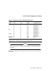
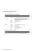
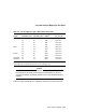
Table 4–7 defines the various PCI_AD fields during the address phase of an
EB164 configuration read/write cycle.
System Address Mapping 4–15