
User`s guide

4.1 Physical Memory Regions
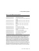
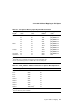
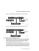
Table 4–1 Three Physical Memory Regions
Region Address Range
16
Description
Cacheable 00.0000.0000–7F.FFFF.FFFF Write-back cached,
load and store merging
operations permitted,
64-byte transfers.
Noncacheable 80.0000.0000–FF.FFEF.FFFF Not cached, load-merging
operations limited, store-
merging operations
permitted, 32-byte
transfers.
Cbox IPR region FF.FFF0.0000–FF.FFFF.FFFF Cbox IPRs. Accesses do
not appear on the interface
pins unless an undefined
location is accessed
(produces UNDEFINED
results).
Table 4–2 provides a more detailed description of the EB164’s address
mapping. The noncached space for EB164 contains the system control and
status registers (CSR’s), noncached memory access (for diagnostics), and
the PCI address space. The PCI defines three physical address spaces: a
4GB PCI memory space, a 4GB PCI I/O space, and a 256-byte-per-device
PCI configuration space. The noncached space is also used to generate PCI
interrupt acknowledge and special cycles.
The 21164 microprocessor has visibility to the complete address space.
However, the PCI devices have a restricted view of the address space. They
can access any PCI device through the PCI memory or I/O space, but they have
no access to the PCI configuration space. The EB164 system provides direct
memory access (DMA) to the system memory through four programmable
windows in the PCI memory space. These address windows are a PCI
requirement. Each window is defined by a base register and is implemented by
all PCI devices.
DMA access to system memory is achieved by either direct-mapped access or
through scatter-gather translation. Direct-mapped accesses are performed by
concatenating an offset to a portion of the PCI address. The scatter-gather
mappings translate any 8KB PCI memory address region into a corresponding
8KB cached memory region.
4–2 System Address Mapping