
User`s guide

4
System Address Mapping
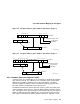
This chapter describes the mapping of the 40-bit processor physical address
space into cacheable and noncacheable memory addresses, the translation
of the processor-initiated address into a peripheral component interconnect
(PCI) space address, and the translation of PCI-initiated addresses into system
memory addresses.
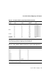
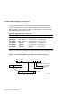
4.1 Physical Memory Regions
The EB164 physical address space, as seen from the 21164, is divided into
three regions:
• Region 1—Cacheable space
• Region 2—Noncacheable space
• Region 3—A region reserved for 21164 cache control and bus interface unit
(Cbox) internal processor registers (IPRs)
In region 1, write-back caching, write-merging operations, and load-merging
operations are all permitted. In regions 2 and 3, load-merging operations are
permitted, but the request includes a mask to tell the system environment
which INT8s are being accessed.
Write-merging operations are also permitted, and the mask indicates which
INT4s are actually modified. The 21164 does not generate accesses to the third
region if they map to a Cbox IPR. Accesses in this region that are not to a
defined Cbox IPR produce UNDEFINED results.
All cacheable accesses by the 21164 microprocessor, as implemented on the
EB164, produce 64-byte requests. All noncacheable (I/O space) references
produce 32-byte requests. Table 4–1 describes each of the three regions.
System Address Mapping 4–1