
User`s guide
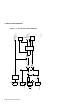


3.10 dc Power Distribution
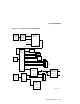
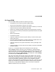
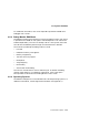
Figure 3–7 SROM and Serial Port
srom_dat
srom_oe_l
PLD
srom_clk
srom_clk_l
test_srom_d_l
J13
eb164.30
eb164.28
21164
eb164.2
SROM
eb164.4
2
5
test_srom_d
eb164.4 MK−2306−17
real_srom_d
MUX
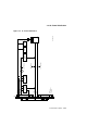
3.10 dc Power Distribution
The EB164 derives its system power from a user-supplied PC power supply.
The power supply must provide +12 V dc and –12 V dc, –5 V dc, +3 V dc,
and Vdd (+5 V dc). The dc power is supplied through power connectors J18
and J29 (eb164.40). (See Figure 3–8.) Power is distributed to the board logic
through dedicated power planes within the 6-layer board structure.
As shown in Figure 3–8, the +12 V dc, –12 V dc, and –5 V dc are supplied to
ISA connectors J19, J20, and J21 (eb164.26). The +12 V dc and –12 V dc are
supplied to ISA connectors and PCI32 connectors J24 and J25 (eb164.22). The
+12 V dc is also supplied to the CPU fan connector J30 (eb164.40), auxiliary
fan connector pins on header J2 (eb164.37), and to the flash ROM write-enable
conector J14 (eb164.33). Vdd is supplied to ISA connectors, PCI32 connectors
and most of the board’s integrated circuits. The +3 V dc is supplied to the
21164 microprocessor.
3–22 Functional Description