
User`s guide
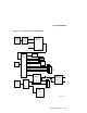
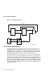

3.7 System Clocks
At system reset, the microprocessor’s irq_h<3:0> pins are driven by the clock
divisor values set by four jumpers on J1. During normal operation, these
signals are used for interrupt requests. The pins are either switched to ground
or pulled up in a specific combination to set the 21164’s internal divider. The
divisor is programmable and can range from 3 to 15. (Refer to Table 2–1 for a
list of jumper combinations.)
The 21164 microprocessor produces the divided clock output signal
sys_clk_out1 that drives the Motorola 88PL117 PLL clock driver chip.
This synchronous system clock provides the system memory and I/O clock
reference.
The clock driver chip is used to minimize system level clock skew as well as
creating square-wave clocks from what can sometimes be an asymmetrical
clock from the 21164. The clock driver provides a 50% duty cycle output clock
that is referenced to the 21164’s sys_clk_out1 and aligned with a reference
feedback clock. The clock driver is configured (OPT<2:0> = 011) such that
the output frequency equals the input frequency and is in phase. The PLL
provides copies to each DSW chip, the CIA chip, each PCI slot, and the
PCI-to-ISA bridge.
The DSW/CIA chipset generates its own 1X and 2X clocks on each ASIC.
Each ASIC uses an integrated PLL together with an onchip clock trunk/buffer
scheme to maintain chip skews under 0.6 ns.
Clock signal sio_clk synchronizes the PCI-to-ISA bridge’s PCI bus
transactions. The supported PCI cycle times range from 40 ns (25 MHz)
to 30 ns (33.3 MHz).
A 14.3-MHz crystal output is buffered through an AV9154-10 frequency
generator to produce the signal osc14. Signal osc14 is routed to the PCI-to-
ISA bridge and the three ISA slots. This is the standard 14.31818-MHz ISA
clock signal.
The frequency generator produces a 24.0-MHz clock (41.7-ns period) osc24.
This signal provides clocking for the 87312 combination controller’s IDE and
diskette data separator.
3–18 Functional Description