
User`s guide

B.5 Bcache Read and Write Timing Calculations
B.5 Bcache Read and Write Timing Calculations
The following sections describe methods of calculating read and write cycle
times.
B.5.1 Read Cycle Calculation
In the 21164, after a Bcache read command begins on CPU cycle N, at time T,
there will be a driver delay Tdd that will slow down the signal and cause it
to appear at the pins at time T + Tdd. There will also be some clock skew of
0.4 ns, delaying some signals until time T + Tdd + 0.4 ns. For the data RAM
output enable, this delay is Taod. When computing BC_RD_SPD, this number
should be taken into account as shown in the following equation:
In other words, the time it takes to perform a Bcache read is the sum of the
times it takes the OE signals to travel out of the CPU (Taod), through the
buffers to the cache SRAMs (Toe2), plus the time to read the SRAMs (Toe), and
the data to get back to the CPU pins (Tdat), plus the data setup time required
by 21164 (Tdsu).
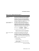
B.5.2 Write Cycle Calculations
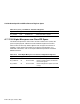
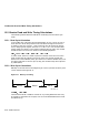
WRsetup is the earliest from the beginning of a write cycle that the write pulse
can be asserted (see Figure B–1).
Figure B–1 Write Cycle Timing
MK−2306−13
WRsetup WRpulse WRhold
The board-level skew is added to account for any timing differences that may
be caused by components in the path, such as the threshold differences inside
the SRAM array.
B–6 SROM Initialization