
User`s guide

B.4 CPU Bus Interface Timing
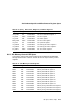
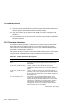
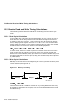
Table B–3 Typical SRAM Specifications
Function Description
Toe Access from OE valid to data valid
Twc Write cycle time
Twp Write pulse width
Tdw Data setup to write pulse deassertion
Tdh Data hold from write pulse deassertion
Taw Address setup to write pulse deassertion
Twr Address hold from write pulse deassertion
Tas Address setup to write pulse assertion
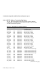
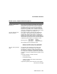
Table B–4 CPU Specifications
Function Description
Taod data_ram_oe_h output delay.
Taoh data_ram_oe_h output hold time.
Tdd Maximum driver delay with 10-pF load (1.6 ns)
Tdod Data output delay = Tdd + 0.4 ns skew.
Tdsu Amount of time required by the 21164 for the data to be ready and
stable before the CPU latches it on the next rising edge of a cycle
(internal CPU setup time).
Tiod Index delay = Tdd + 0.4 ns skew.
SROM Initialization B–5