
User`s guide

A.3 PCI Dense Memory Space
A.3.3 Flash ROM Configuration Registers
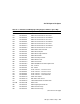
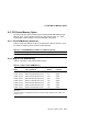
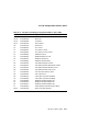
Table A–10 lists the configuration registers for the Intel 28F008SA 1MB flash
ROM. A read operation is performed by reading from the appropriate address.
To write data, the flash ROM must first be erased. The structure of the
flash ROM allows only the flash ROM to be erased in 64KB blocks (see
Section A.3.2).
In order to change one byte, the following steps must be completed:
1. Read the entire 64KB block into system memory.
2. Change the desired byte in system memory.
3. Erase the 64KB block in flash ROM.
4. Write the entire 64KB block from system memory to the flash ROM.
Note
In order to write to flash ROM, Jumper J14 (protect/enable) must be
positioned on pins 2 and 3 (see Table 2–1 and schematic eb164.33).
All flash ROM accesses (except for read operations) require two bus cycles.
During the first cycle, register data is written to set up the registers. During
the second cycle, the read or write transaction performs the operation desired.
For more information about reading, erasing, and writing the flash ROM, see
the Intel Flash Memory document.
Accessing the flash ROM registers requires byte access, which is only possible
through use of PCI sparse memory space. The EB164 flash ROM resides in
PCI memory address range FFF8.0000 to FFFF.FFFF. See Section 4.2.2 for
information about accessing this address range through sparse memory space.
A–14 I/O Space Address Maps