
Data Sheet


2/10/2018 Zybo Z7 Reference Manual [Reference.Digilentinc]
https://reference.digilentinc.com/reference/programmable-logic/zybo-z7/reference-manual 19/33
The Zybo Z7 provides a 33.3333 MHz () clock to the Zynq PS_CLK input, which is used to generate the clocks for each of the PS
subsystems. The 33.3333 MHz () input allows the processor to operate at a maximum frequency of 667 MHz () and the DDR3 memory
controller to operate at a maximum clock rate of 533 MHz () (1066 MT/s). The Zybo Z7 board files, available on the Zybo Z7 Resource
Center (https://reference.digilentinc.com/reference/programmable-logic/zybo-z7/start), will automatically configure the Zynq processing system
IP core in Vivado to work with all PS attached devices, including the 33.3333 MHz () input oscillator.
The PS has a dedicated PLL capable of generating up to four reference clocks, each with settable frequencies, that can be used to clock
custom logic implemented in the PL. Additionally, The Zybo Z7 provides an external 125 MHz () reference clock directly to pin K17 of the
PL. The external reference clock allows the PL to be used completely independently of the PS, which can be useful for simple applications
that do not require the processor.
The PL of the Zynq-Z7010 also includes two MMCM’s and two PLL’s that can be used to generate clocks with precise frequencies and
phase relationships. Any of the four PS reference clocks or the 125 MHz () external reference clock can be used as an input to the MMCMs
and PLLs. For a full description of the capabilities of the Zynq PL clocking resources, refer to the “7 Series FPGAs Clocking Resources
User Guide” available from Xilinx.
Xilinx offers the Clocking Wizard IP core to assist in integrating the MMCM's and PLL's into a design. This wizard will properly instantiate
the needed MMCMs and PLLs based on the desired frequencies and phase relationships specified by the user. The wizard will then output
an easy-to-use wrapper component around these clocking resources that can be inserted into the user’s design. The clocking wizard can be
accessed from within the Vivado and IP Integrator tools.
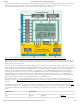
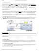
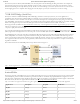
Figure 5.1 outlines the clocking scheme used on the Zybo Z7. Note that the reference clock output from the Ethernet PHY is used as the
125 MHz () reference clock to the PL, in order to cut the cost of including a dedicated oscillator for this purpose. Keep in mind that
CLK125 will be disabled when the Ethernet PHY is held in hardware reset by driving the PHYRSTB signal low.
(https://reference.digilentinc.com/_detail/reference/programmable-logic/zybo-z7/zybo-z7-clock.png?id=reference%3Aprogrammable-logic%3Azybo-
z7%3Areference-manual)
Figure 5.1. Zybo Z7 clocking.
The Zybo Z7 provides several different methods of resetting the Zynq-7000 device, as described in the following sections.
The Zynq PS supports external power-on reset signals. The power-on reset is the master reset of the entire chip. This signal resets every
register in the device capable of being reset. The Zybo Z7 drives this signal from the PWRGD signal of the ADP5052 power regulator in
order to hold the system in reset until all power supplies are valid.
A red push button, labeled PROGB, toggles the Zynq-7000's PROG_B input. This resets the PL and causes DONE to be de-asserted. The
PL will remain unconfigured until it is reprogrammed by the processor or via JTAG.
5 Oscillators/Clocks
6 Reset Sources
6.1 Power-on Reset
6.2 Programmable Logic Reset
6.3 Processor Subsystem Reset