
Data Sheet


2/10/2018 Zybo Z7 Reference Manual [Reference.Digilentinc]
https://reference.digilentinc.com/reference/programmable-logic/zybo-z7/reference-manual 18/33
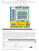
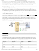
The Zybo Z7 includes two Micron MT41K256M16HA-125 DDR3L memory components creating a single rank, 32-bit wide interface and a
total of 1 GiB (Gibi-byte, or 1,073,741,824 bytes) of capacity. The DDR3L is connected to the hard memory controller in the Processor
Subsystem (PS), as outlined in the Zynq documentation.
The PS incorporates an AXI memory port interface, a DDR controller, the associated PHY, and a dedicated I/O bank. DDR3L memory
interface speeds up to 533 MHz ()/1066 Mbps are supported.
Zybo Z7 was routed with 40 ohm (+/-10%) trace impedance for single-ended signals, and differential clock and strobes set to 80 ohms
(+/-10%). A feature called DCI (Digitally Controlled Impedance) is used to match the drive strength and termination impedance of the PS
pins to the trace impedance. On the memory side, each chip calibrates its on-die termination and drive strength using a 240 ohm resistor on
the ZQ pin.
Due to layout reasons, the two lower data byte groups (DQ[0-7], DQ[8-15]) were swapped. To the same effect, the data bits inside byte
groups were swapped as well. These changes are transparent to the user. During the whole design process the Xilinx PCB guidelines were
followed.
Both the memory chips and the PS DDR bank are powered from the 1.35V supply. The mid-point reference of 0.675V is created with a
simple resistor divider and is available to the Zynq as external reference.
For proper operation it is essential that the PS memory controller is configured properly. Settings range from the actual memory flavor to
the board trace delays. For your convenience, the Zybo Z7 Vivado board files are available on the Zybo Z7 Resource Center
(https://reference.digilentinc.com/reference/programmable-logic/zybo-z7/start) and automatically configure the Zynq Processing System IP core
with the correct parameters.
For best DDR3L performance, DRAM training is enabled for write leveling, read gate, and read data eye options in the PS Configuration
Tool in Xilinx tools. Training is done dynamically by the controller to account for board delays, process variations and thermal drift.
Optimum starting values for the training process are the board delays (propagation delays) for certain memory signals.
Board delays are specified for each of the byte groups. These parameters are board-specific and were calculated from the PCB trace length
reports. The DQS to CLK Delay and Board Delay values are calculated specific to the Zybo Z7 memory interface PCB design.
For more details on memory controller operation, refer to the Xilinx Zynq Technical Reference manual
(http://www.xilinx.com/support/documentation/user_guides/ug585-Zynq-7000-TRM.pdf).
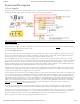
The Zybo Z7 features a Spansion S25FL128S 4-bit Quad-SPI serial NOR flash. The key device attributes are:
Part number S25FL128S
16 MiB (16,777,216 bytes)
1-bit, 2-bit, and 4-bit bus widths supported
General use clock speeds up to 100 MHz (), translating to 400 Mbps in Quad-SPI mode
Zynq configuration clock speeds up to 94 MHz ().
Powered from 3.3V
The Flash memory is used to provide non-volatile code and data storage. It can be used to initialize the PS and PL of the Zynq device with a
Zynq Boot Image (also known as BOOT.BIN) generated using Xilinx tools such as Petalinux or Xilinx SDK. For information on booting
the Zybo Z7 with a Zynq Boot image, see section “2.2 Quad SPI Boot Mode”.
The Flash is also commonly used to store non-configuration data needed by the application. If doing this from a bare-metal application, The
flash memory can be freely accessed using standalone libraries included with a Xilinx SDK BSP project. If doing this from a Petalinux
generated embedded Linux system, the Flash can be partitioned as desired and mounted/accessed like a standard MTD block device. See
the Petalinux and Xilinx SDK documentation for more information.
The Flash connects to the Quad-SPI Flash controller of the Zynq-7000 PS via pins in MIO Bank 0/500 (specifically MIO[1:6,8]), as
outlined in the Zynq Technical Reference Manual. Quad-SPI feedback mode is used, thus qspi_sclk_fb_out/MIO[8] is left to freely toggle
and is connected only to a 20K pull-up resistor to 3.3V. This allows a Quad-SPI clock frequency greater than FQSPICLK2. The details of
these connections do not need to be known when using the Zybo Z7 Vivado Board files, as they will automatically configure your project to
work correctly with the on-board Flash.
A globally unique MAC address is programmed into the One-Time-Programmable (OTP) region of the Flash on each Zybo Z7 at the
factory. For more information on this, see section “10 Ethernet”.
The OTP region also includes a factory-programmed read-only 128-bit random number. The very lowest address range [0x00;0x0F] can be
read to access the random number. See the Spansion S25FL128S datasheet for information on this random number and accessing the OTP
region.
4 Quad-SPI Flash