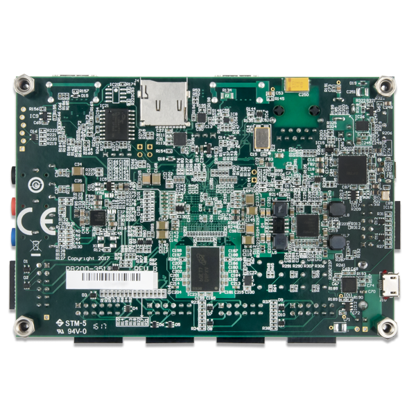
2/10/2018 Zybo Z7 Reference Manual [Reference.Digilentinc] Zybo Z7 Reference Manual The Zybo Z7 is a feature-rich, ready-to-use embedded software and digital circuit development board built around the Xilinx Zynq-7000 family. The Zynq family is based on the Xilinx All Programmable System-on-Chip (AP SoC) architecture, which tightly integrates a dualcore ARM Cortex-A9 processor with Xilinx 7-series Field Programmable Gate Array (FPGA) logic.
/10/2018 Zybo Z7 Reference Manual [Reference.Digilentinc] https://reference.digilentinc.
2/10/2018 Zybo Z7 Reference Manual [Reference.Digilentinc] https://reference.digilentinc.
2/10/2018 Zybo Z7 Reference Manual [Reference.Digilentinc] https://reference.digilentinc.
2/10/2018 Zybo Z7 Reference Manual [Reference.Digilentinc] https://reference.digilentinc.
2/10/2018 Zybo Z7 Reference Manual [Reference.Digilentinc] https://reference.digilentinc.
2/10/2018 Zybo Z7 Reference Manual [Reference.Digilentinc] Download This Reference Manual Zybo Z7 PDF (https://reference.digilentinc.com/_media/reference/programmable-logic/zybo-z7/zybo-z7_rm.pdf) Features ZYNQ Processor 667 MHz () dual-core Cortex-A9 processor DDR3L memory controller with 8 DMA channels and 4 High Performance AXI3 Slave ports High-bandwidth peripheral controllers: 1G Ethernet, USB 2.
2/10/2018 Zybo Z7 Reference Manual [Reference.Digilentinc] HDMI sink port (input) with/without* CEC HDMI source port (output) with CEC Audio codec with stereo headphone, stereo line-in, and microphone jacks Switches, Push-buttons, and LEDs 6 push-buttons (2 processor connected) 4 slide switches 5 LEDs (1 processor connected) 2 RGB LEDs (1*) Expansion Connectors 6 Pmod ports (5*) 8 Total Processor I/O 40 Total FPGA I/O (32*) 4 Analog capable 0-1.
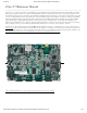
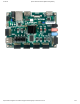
2/10/2018 Zybo Z7 Reference Manual [Reference.Digilentinc] Callout Description Callout Description Callout Description 5 MIO Pmod port 16 Audio codec ports 27 Power supply good LED () 6 USB 2.
2/10/2018 Zybo Z7 Reference Manual [Reference.Digilentinc] Product Variant Zybo Z7-10 Zybo Z7-20 Flip-Flops 35,200 106,400 Block RAM () 270 KB 630 KB Clock Management Tiles 2 4 Total Pmod ports 5 6 Fan connector No Yes Zynq heat sink No Yes HDMI CEC Support TX port only TX and RX ports RGB LED () 1 2 The Zybo Z7-20 includes a heat sink in order to dissipate the extra heat generated from the additional FPGA resources when running complex, fast-switching designs.
2/10/2018 Zybo Z7 Reference Manual [Reference.Digilentinc] The Zynq APSoC is divided into two distinct subsystems: The Processing System (PS) and the Programmable Logic (PL). The figure below shows an overview of the Zynq APSoC architecture, with the PS colored light green and the PL in yellow. Note that the PCIe Gen2 controller and Multi-gigabit transceivers are not available on the Zynq-7020 or Zynq-7010 devices. (https://reference.digilentinc.com/_detail/zybo/zyng1.
2/10/2018 Zybo Z7 Reference Manual [Reference.Digilentinc] 0 JF7 1 CS () 2 DQ0 3 DQ1 4 DQ2 5 DQ3 6 SCLK () 7 LED4 8 SCLK () FB 9 JF8 10 JF2 11 JF3 12 JF4 13 JF1 14 JF9 15 JF10 MIO 501 1.8V Pin Peripherals ENET 0 16 TXCK 17 TXD0 18 TXD1 19 TXD2 20 TXD3 21 TXCTL 22 RXCK 23 RXD0 24 RXD1 25 RXD2 26 RXD3 USB 0 SDIO 0 https://reference.digilentinc.
2/10/2018 27 Zybo Z7 Reference Manual [Reference.Digilentinc] RXCTL 28 DATA4 29 DIR 30 STP 31 NXT 32 DATA0 33 DATA1 34 DATA2 35 DATA3 36 CLK 37 DATA5 38 DATA6 39 DATA7 40 CCLK 41 CMD 42 D0 43 D1 44 D2 45 D3 46 RESETN 47 CD 48 RXD (output) 49 TXD (input) 50 BTN4 51 BTN5 52 MDC 53 MDIO https://reference.digilentinc.
2/10/2018 Zybo Z7 Reference Manual [Reference.Digilentinc] Functional Description 1 Power Supplies The Zybo Z7 power circuitry was carefully designed to meet the requirements of the Zynq-7000 and all other peripherals while also providing flexible input supply options. An overview of the power circuit is shown in Figure 1.1. (https://reference.digilentinc.com/_detail/reference/programmable-logic/zybo-z7/zybo-z7-power.png?id=reference%3Aprogrammable-logic%3Azyboz7%3Areference-manual) Figure 1.1.
2/10/2018 Zybo Z7 Reference Manual [Reference.Digilentinc] Connector Type JP6 Configuration Connector Label Schematic net name Min/Rec/Max Voltage (V) Current Limit (A) Barrel jack WALL J17 VJACK 4.5/5/5.5 4.0 Battery/Other BAT JP6, J16 VU5V0 4.5/5/5.5 4.0 USB USB J12 VBUS See USB specification 0.75 Table 1.1.1. Zybo Z7 Power Input Specifications 1.2 Power Specifications Table 1.2.1 describes the characteristics the Zybo Z7's on-board power rails.
2/10/2018 Zybo Z7 Reference Manual [Reference.Digilentinc] Once a 12-bit value is obtained from the XADC, you can use the equation in Figure 1.4.1 to convert it to current consumption. X is the 12bit value from the XADC and I is the current consumption in Amps. Be careful not to use the 16-bit value obtained directly from the XADC registers with this equation; it needs to be right-shifted by four in order to ignore the four least significant bits. (https://reference.digilentinc.
2/10/2018 Zybo Z7 Reference Manual [Reference.Digilentinc] (https://reference.digilentinc.com/_detail/reference/programmable-logic/zybo-z7/zybo-z7-config.png?id=reference%3Aprogrammable-logic%3Azyboz7%3Areference-manual) Figure 2.1. Zybo Z7 configuration pins. The three boot modes are described in the following sections. 2.1 microSD Boot Mode The Zybo Z7 supports booting from a microSD card inserted into connector J4.
2/10/2018 Zybo Z7 Reference Manual [Reference.Digilentinc] The Zybo Z7 includes two Micron MT41K256M16HA-125 DDR3L memory components creating a single rank, 32-bit wide interface and a total of 1 GiB (Gibi-byte, or 1,073,741,824 bytes) of capacity. The DDR3L is connected to the hard memory controller in the Processor Subsystem (PS), as outlined in the Zynq documentation. The PS incorporates an AXI memory port interface, a DDR controller, the associated PHY, and a dedicated I/O bank.
2/10/2018 Zybo Z7 Reference Manual [Reference.Digilentinc] 5 Oscillators/Clocks The Zybo Z7 provides a 33.3333 MHz () clock to the Zynq PS_CLK input, which is used to generate the clocks for each of the PS subsystems. The 33.3333 MHz () input allows the processor to operate at a maximum frequency of 667 MHz () and the DDR3 memory controller to operate at a maximum clock rate of 533 MHz () (1066 MT/s). The Zybo Z7 board files, available on the Zybo Z7 Resource Center (https://reference.digilentinc.
2/10/2018 Zybo Z7 Reference Manual [Reference.Digilentinc] The external system reset button, labeled PS-SRST, resets the Zynq device without disturbing the debug environment. For example, the previous break points set by the user remain valid after system reset. Due to security concerns, system reset erases all memory content within the PS, including the On-Chip-Memory (OCM). The PL is also cleared during a system reset. System reset does not cause the boot mode strapping pins to be re-sampled.
2/10/2018 Zybo Z7 Reference Manual [Reference.Digilentinc] SD_CCLK Clock MIO40 5 SD_CMD Command MIO41 3 SD_CD Card Detect MIO47 9 Table 8.1. MicroSD pinout The SD slot is powered from 3.3V, but is connected through MIO Bank 1/501 (1.8V). Therefore, a TI TXS02612 level shifter performs this translation. The TXS02612 is actually a 2-port SDIO port expander, but only its level shifter function is used. The connection diagram can be seen on Figure 8.1.
2/10/2018 Zybo Z7 Reference Manual [Reference.Digilentinc] Note that if your project uses the USB host feature (embedded or general purpose), then the Zybo Z7 is very likely to consume more current than is allowed by a USB peripheral, causing it to periodically reset. When this occurs the PGOOD LED () will quickly flicker and the DONE LED () will go low, indicating the PL is no longer programmed. To prevent this, power the Zybo Z7 by a 5V battery or wall adapter capable of providing more power.
2/10/2018 Zybo Z7 Reference Manual [Reference.Digilentinc] Table 10.1. Ethernet status LEDs The Zynq incorporates two independent Gigabit Ethernet Controllers. They implement a 10/100/1000 half/full duplex Ethernet MAC. Of these two, GEM 0 can be mapped to the MIO pins where the PHY interfaces. Since the MIO bank is powered from 1.8V, the RGMII interface uses 1.8V HSTL Class 1 drivers. For this I/O standard an external reference of 0.9V is provided in bank 501 (PS_MIO_VREF).
2/10/2018 Zybo Z7 Reference Manual [Reference.Digilentinc] CLK_P, CLK_N Clock output H16, H17 Clock input U18, U19 CEC Consumer Electronics Control bidirectional (optional) E19 CEC bidirectional (optional, N/A on Zybo Z7-10) Y8 SCL, SDA DDC bidirectional (optional) G17, G18 DDC bidirectional W18, Y19 HPD/HPA Hot-plug detect input (inverted, optional) E18 Hot-plug assert output W19 Table 11.1. HDMI pin description and assignment 11.
2/10/2018 Zybo Z7 Reference Manual [Reference.Digilentinc] SSM2603 pin Protocol Direction from Zynq Zynq pin BCLK I²S (Serial Clock) Output R19 PBDAT I²S (Playback Data) Output R18 PBLRC I²S (Playback Channel Clock) Output T19 RECDAT I²S (Record Data) Input R16 RECLRC I²S (Record Channel Clock) Output Y18 SDIN I²C (Data) Input/Output N17 SCLK () I²C (Clock) Output N18 MUTE Digital Enable (Active Low) Output P18 MCLK Master Clock Output R17 Table 12.2.
2/10/2018 Zybo Z7 Reference Manual [Reference.Digilentinc] resistors to prevent damage from inadvertent short circuits (a short circuit could occur if a pin assigned to a push-button or slide switch was inadvertently defined as an output). The push-buttons are “momentary” switches that normally generate a low output when they are at rest, and a high output only when they are pressed. Slide switches generate constant high or low inputs depending on their position. (https://reference.digilentinc.
2/10/2018 Zybo Z7 Reference Manual [Reference.Digilentinc] 14 Fan The Zybo Z7-20 has a connector that can be used to power a fan mounted to the included heat sink. Digilent sells a 5V fan suitable for this purpose. In order to attach the fan to the Zybo Z7-20 heat sink, two of the included screws must be tightened into the space between the heat sink fins (the heat sink does not contain mounting holes).
2/10/2018 Zybo Z7 Reference Manual [Reference.Digilentinc] (https://reference.digilentinc.com/_detail/reference/programmable-logic/zybo-z7/fan_fig.png?id=reference%3Aprogrammable-logic%3Azyboz7%3Areference-manual) Figure 14.2. Fan Speed Feedback Signal It is possible to monitor the temperature of the Zynq device during operation over JTAG from the hardware server in Vivado. The maximum recommended operating temperature for the Zynq-7020 device is 85°C.
2/10/2018 Zybo Z7 Reference Manual [Reference.
2/10/2018 Zybo Z7 Reference Manual [Reference.Digilentinc] The MIPI CSI-2 bus is passively terminated on the Zybo Z7 and connected directly to the Zynq PL. The guidelines described in Xilinx application note XAPP894 D-PHY solutions (https://www.xilinx.com/support/documentation/application_notes/xapp894-d-phy-solutions.pdf) were followed in order to implement a compatible D-PHY receiver using the Zynq. The interface is tested to operate at up to 672 Mbps on each lane.
2/10/2018 Zybo Z7 Reference Manual [Reference.Digilentinc] Table 16.1. Zybo Z7 Pmod Pinout 16.1 Standard Pmod The standard Pmod ports are connected to the Zynq PL via 200 Ohm series resistors. The series resistors prevent short circuits that can occur if the user accidentally drives a signal that is supposed to be used as an input. The downside to this added protection is that these resistors can limit the maximum switching speed of the data signals.
2/10/2018 Zybo Z7 Reference Manual [Reference.Digilentinc] Email ddress Submit Our Partners Xilinx University Program Help Customer Info Technical Support Forum Videos Company Info About Us (https://youtube.com/user/digilentinc)(https://store.digilentinc.com/p (https://store.digilentinc.com/partners/xilinx(https://forum.digilentinc.com) FAQ pageid=26) university-program/) Reference Wiki (https://resource.digilentinc.com/verify/faq) Shipping & Returns (https://reference.digilentinc.
2/10/2018 Zybo Z7 Reference Manual [Reference.Digilentinc] (https://www.reddit.com/r/digilent) (https://www.linkedin.com/company/1454013) (https://www.flickr.com/photos/127815101@N07) https://reference.digilentinc.


