
Data Sheet

PmodPMON1™ Manual
Copyright Digilent, Inc. All rights reserved.
Other product and company names mentioned may be trademarks of their respective owners.
Page 2 of 2
3 Device Configuration
For specific information related to device configuration on the AD5112 and ADM1191, please refer to the data
sheets available at www.analog.com
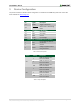
Connector J1 – Control Pins
Pin
Signal
Description
1,2
CONV
Trigger a conversion
3,4
ALERT
Overcurrent or overvoltage
event
Connector J2 – I2C Interface
1,2
SCL
Serial Clock
3,4
SDA
Serial Data
5,6
GND
Ground
7,8
DVDD
Input Voltage
Connector J3 – Power Monitor Screw Terminal
1
VIN
Input voltage of device to
monitored
2
GND
Ground
3
VOUT
Voltage supplied to device
being monitored
Table 1. Connector descriptions.
Table 2. Jumper descriptions.
Jumper
Setting
Description
JP1
1
ADM1191 Address bit 3
and 2 set to 0b00
3
ADM1191 Address bit 3
and 2 set to 0b01
OFF
ADM1191 Address bit 3
and 2 set to 0b10
JP2
1
ADM1191 Address bit 1
and 0 set to 0b00
3
ADM1191 Address bit 1
and 0 set to 0b01
OFF
ADM1191 Address bit 1
and 0 set to 0b10